Beyond Rth(j-c): A Practical Engineer’s Guide to IGBT Module Junction Temperature Estimation and Heatsink Design
In the world of power electronics, the datasheet value for Junction-to-Case Thermal Resistance, Rth(j-c), is often the first—and sometimes only—metric engineers consider for thermal management. While fundamental, relying solely on this value is like navigating with only one star in the sky. True thermal design mastery requires a deeper understanding of the entire thermal pathway, from the silicon chip to the ambient air. Overlooking any part of this chain can lead to systems that underperform, age prematurely, or fail catastrophically under real-world load conditions.
This guide moves beyond a single datasheet parameter to provide a comprehensive, practical framework for estimating IGBT junction temperature (Tj) and designing an effective cooling solution. We’ll break down the thermal resistance network, walk through power loss calculations, and apply these principles to a step-by-step heatsink selection process, ensuring your power systems are not just functional, but robust and reliable. For a deeper look into why thermal resistance is a critical parameter, explore our analysis on Why Rth Matters: Unlocking IGBT Thermal Performance.
Deconstructing the Thermal Resistance Network: From Chip to Ambient Air
Think of heat flowing from the IGBT junction to the outside world as current moving through a series of resistors. Each layer in the physical assembly presents an opposition to heat flow, which we quantify as thermal resistance, measured in °C/W or K/W. The total temperature rise is the sum of the temperature drops across each of these thermal resistors.
The Meaning of Rth(j-c): Junction-to-Case Thermal Resistance
Rth(j-c) represents the thermal resistance between the semiconductor chip’s active junction and the module’s case or baseplate. This value is determined entirely by the module’s internal construction—the die attach method, the ceramic substrate material (e.g., Al2O3, AlN), and the baseplate material. A lower Rth(j-c) indicates a more efficient internal heat transfer path. For example, the SKM300GB128D, with its standard screw-terminal package and copper baseplate, is designed for low Rth(j-c) to handle significant power dissipation.
The Critical Middle Layers: Rth(c-s) and the Role of Thermal Interface Material (TIM)
Rth(c-s), or Case-to-Sink thermal resistance, is one of the most critical and often underestimated variables in the thermal equation. It represents the resistance at the interface between the module’s baseplate and the heatsink. Even surfaces that appear perfectly flat have microscopic imperfections that trap air, a poor conductor of heat.
To overcome this, a Thermal Interface Material (TIM) such as thermal grease or a phase-change pad is applied. The effectiveness of the TIM, its thickness, and the mounting pressure all directly impact Rth(c-s). In fact, a poorly applied TIM can contribute to over 50% of the total thermal resistance from the chip to the heatsink, creating a bottleneck that renders an expensive, high-performance heatsink ineffective.
The Final Hurdle: Rth(s-a) and Heatsink Performance
Rth(s-a) is the thermal resistance from the heatsink to the ambient air. This value is a function of the heatsink’s design (material, surface area, fin geometry) and the cooling method (natural convection vs. forced air). A larger heatsink with a powerful fan will have a much lower Rth(s-a) than a small, passively cooled one. Your choice here is a trade-off between thermal performance, physical size, cost, and system complexity.
Key Takeaways: The total thermal resistance is a chain of Rth(j-c) + Rth(c-s) + Rth(s-a). The Rth(j-c) is fixed by the module manufacturer, but you, the design engineer, have direct control over Rth(c-s) through TIM selection and application, and Rth(s-a) through heatsink choice. The entire chain is only as strong as its weakest link.
The Core of the Calculation: Estimating Total Power Loss (P_total)
To use the thermal resistance network, you must first determine the amount of heat being generated. The total power loss (P_total) in an IGBT module is primarily the sum of conduction losses and switching losses.
Calculating Conduction Losses (P_cond)
Conduction losses occur when the IGBT is in the “on” state, conducting current. They are calculated based on the collector-emitter saturation voltage (Vce(sat)) and the collector current (Ic). The Vce(sat) is not constant; it depends on both the collector current and the junction temperature. Datasheets provide curves showing this relationship.
A simplified formula for average conduction loss in a PWM inverter application is:
P_cond = Vce(sat) * I_avg * D
Where I_avg is the average current during the on-time and D is the duty cycle.
Calculating Switching Losses (P_sw)
Switching losses occur during the transitions between the “on” and “off” states. During these brief intervals, both voltage across the device and current through it are high, leading to a spike in power dissipation. These losses are directly proportional to the switching frequency (f_sw).
Datasheets typically provide energy loss values for turn-on (Eon) and turn-off (Eoff) under specific test conditions. The total switching loss can be calculated as:
P_sw = (Eon + Eoff) * f_sw
It’s crucial to adjust the datasheet Eon and Eoff values for your specific DC bus voltage, collector current, and gate drive conditions, as these parameters significantly affect switching losses.
Bringing It All Together: P_total = P_cond + P_sw
The total power dissipated as heat by the IGBT is the sum of these two components. Remember to perform this calculation for both the IGBT and the anti-parallel diode, as both contribute to the module’s total heat generation. For a comprehensive guide on how module construction impacts these factors, see our article on how IGBT packaging dictates thermal performance.
Key Takeaways: Power loss calculation is fundamental to thermal design. Conduction losses dominate in low-frequency, high-current applications, while switching losses become the major contributor at higher frequencies. Accurately estimating P_total is the first step toward selecting the right heatsink.
A Practical Walkthrough: Heatsink Selection for an IGBT Module
Let’s apply these concepts to a real-world scenario. The goal is to select a heatsink that keeps the IGBT junction temperature (Tj) below its maximum rating (typically 150°C or 175°C) with a safety margin.
Step 1: Define Your Operating Conditions and Power Losses
- Maximum ambient temperature (Ta_max): e.g., 50°C
- Maximum desired junction temperature (Tj_max): e.g., 125°C (providing a 25°C safety margin below a 150°C limit)
- Total calculated power loss (P_total): e.g., 250 W (per module)
- Datasheet Rth(j-c) for the IGBT: e.g., 0.08 °C/W
- Estimated Rth(c-s) with good quality thermal paste: e.g., 0.03 °C/W
Step 2: Calculate the Maximum Allowable Heatsink Thermal Resistance (Rth(s-a)_max)
The total temperature rise from ambient to junction is given by:
Tj_max - Ta_max = P_total * (Rth(j-c) + Rth(c-s) + Rth(s-a))
Rearranging the formula to solve for the required heatsink resistance:
Rth(s-a)_max = ((Tj_max - Ta_max) / P_total) - Rth(j-c) - Rth(c-s)
Plugging in our values:
Rth(s-a)_max = ((125°C - 50°C) / 250 W) - 0.08 °C/W - 0.03 °C/W
Rth(s-a)_max = (75°C / 250 W) - 0.11 °C/W
Rth(s-a)_max = 0.3 °C/W - 0.11 °C/W = 0.19 °C/W
This result is your target. You must select a heatsink with a thermal resistance of 0.19 °C/W or lower to meet your design goals.
Step 3: Selecting the Right Heatsink and Verifying Performance
With your calculated Rth(s-a)_max, you can now consult heatsink manufacturer catalogs. You will find charts that plot thermal resistance against airflow (in LFM or m/s) for forced convection heatsinks, or against power dissipation for natural convection. Select a heatsink that provides a value at or below 0.19 °C/W under your system’s airflow conditions.
Case Study Contrast: Standard vs. Baseplate-less Modules
The thermal design strategy changes significantly with module packaging. Let’s compare two types:
| Feature | Standard Module (e.g., SKM300GB128D) | Baseplate-less Module (e.g., FP50R12KE3) |
|---|---|---|
| Structure | Features a thick copper baseplate for heat spreading. | The ceramic substrate (DBC) mounts directly to the heatsink. |
| Heat Path | Die → Substrate → Baseplate → TIM → Heatsink. The baseplate spreads heat effectively. | Die → Substrate → TIM → Heatsink. A more direct but concentrated heat path. |
| Rth(j-c) vs Rth(j-s) | Rth(j-c) is well-defined. Overall performance relies heavily on low Rth(c-s). | Rth(j-s) (junction-to-sink) is the critical parameter. Heat spreading is less effective, making the TIM layer and heatsink flatness crucial. |
| Design Consideration | Tolerant of minor heatsink surface imperfections due to the rigid baseplate. | Requires a very flat heatsink surface and carefully controlled TIM application to avoid hotspots and mechanical stress on the substrate. |
The choice between these packages depends on the application’s cost, power density, and reliability requirements. While baseplate-less modules like the FP50R12KE3 can offer a lower total thermal resistance in an optimized design, they demand more stringent control over the mechanical and thermal interface. For further reading, consult authoritative resources on thermal management and specific IGBT modules.
Key Takeaways: Heatsink selection is a methodical process of defining limits, calculating losses, and determining the required thermal resistance. The module’s packaging technology dictates the specific thermal challenges and design priorities, particularly regarding the interface to the heatsink.
Common Pitfalls and Expert Tips in Thermal Design
Even with perfect calculations, poor implementation can ruin a thermal design. Here are common issues seen in the field:
- The Hidden Dangers of Poor TIM Application: Applying too much TIM increases the Rth(c-s) layer thickness, impeding heat flow. Applying too little, or unevenly, creates voids filled with air, leading to dangerous hotspots. Using a stencil for screen printing provides the most consistent and reliable results.
- Uneven Mounting Pressure: Failure to follow the manufacturer’s specified torque values and tightening sequence can cause the module baseplate to warp. This creates gaps in the TIM layer, dramatically increasing thermal resistance and potentially leading to substrate cracks over time.
- Derating for High Altitude and Enclosed Environments: Standard heatsink performance data is based on sea-level air density. At higher altitudes, the thinner air is less effective at removing heat, requiring a larger heatsink or more powerful fan. Similarly, if the module is in a poorly ventilated enclosure, the local “ambient” temperature will be much higher than the room temperature, a factor that must be included in your initial Ta_max assumption.
Conclusion: A Holistic Approach to IGBT Thermal Management
Effective thermal design is not about a single number; it’s about managing the entire chain of thermal resistances from the semiconductor junction to the ambient environment. While Rth(j-c) is the starting point provided by the module manufacturer, the engineer’s true value lies in optimizing the external factors: selecting the appropriate Thermal Interface Material, ensuring its meticulous application, and choosing a heatsink that meets the calculated Rth(s-a) requirement for worst-case operating conditions. By embracing this holistic approach and paying close attention to both calculation and implementation, you can design high-power systems that operate reliably and deliver their full performance potential for their entire intended lifespan.
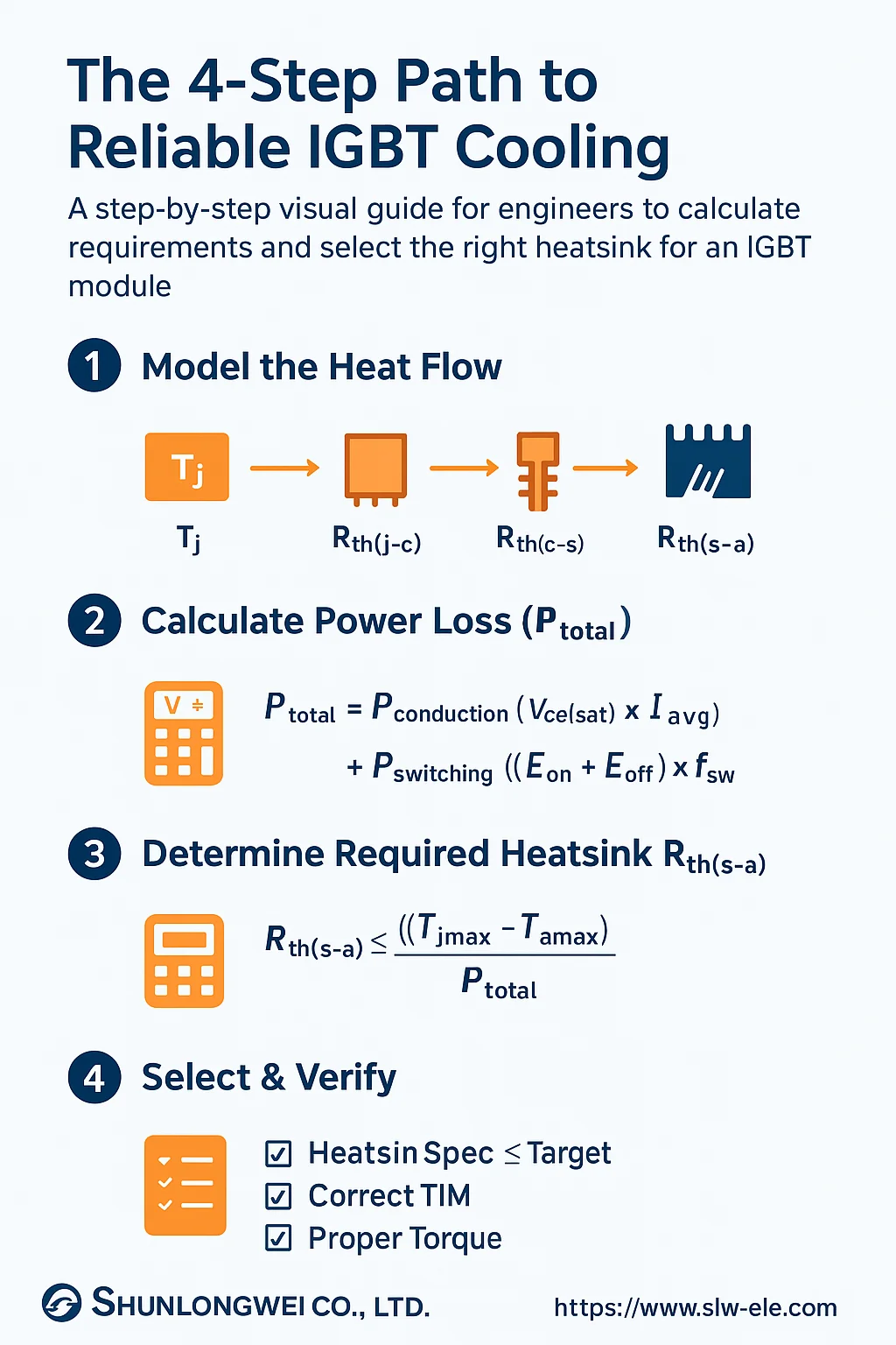
Infographic: Mastering IGBT Thermal Design
- Title: The 4-Step Path to Reliable IGBT Cooling
- Core Concept: A step-by-step visual guide for engineers to calculate requirements and select the right heatsink for an IGBT module.
- Key Sections & Visuals:
- Point 1: Model the Heat Flow.
- Content: Visualize the thermal resistance chain: Tj → Rth(j-c) → Tc → Rth(c-s) → Ts → Rth(s-a) → Ta.
- Icon Concept: A simple diagram showing a chip, a case, a heatsink, and arrows representing heat flow through resistors.
- Point 2: Calculate Power Loss (P_total).
- Content: P_total = P_conduction (Vce(sat) x I_avg) + P_switching ((Eon+Eoff) x f_sw). Highlight that high frequency increases switching loss.
- Icon Concept: A simple formula visualization with icons for current, voltage, and a frequency wave.
- Point 3: Determine Required Heatsink Rth(s-a).
- Content: Rth(s-a) ≤ ((Tj_max – Ta_max) / P_total) – Rth(j-c) – Rth(c-s). Emphasize setting a safety margin for Tj_max.
- Icon Concept: A calculator icon next to the core formula, with input fields for Tj, Ta, and P.
- Point 4: Select & Verify.
- Content: Compare your required Rth(s-a) with manufacturer data. Crucial factors: TIM quality, mounting torque, and airflow.
- Icon Concept: A checklist icon with items: “Heatsink Spec ≤ Target,” “Correct TIM,” “Proper Torque.”
- Point 1: Model the Heat Flow.
- Branding: Include Logo: Shunlongwei Co., Ltd. | Website: https://www.slw-ele.com
Related Articles:
- https://www.slw-ele.com/resources/the-core-trio-of-igbt-module-selection-a-practical-guide-to-voltage-current-and-thermal-management
- https://www.slw-ele.com/mastering-igbt-paralleling-a-guide-to-achieving-balanced-current-sharing.html
- https://www.slw-ele.com/ipm-vs-discrete-igbt-a-framework-for-system-cost-and-reliability.html
- https://www.slw-ele.com/from-chip-to-air-a-holistic-approach-to-igbt-thermal-design.html