Content last revised on October 11, 2026
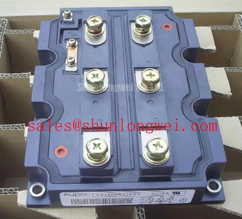
FZ1800R17HE4_B9 Infineon 1700V 1800A IGBT Module
With the DC link fully isolated, discharged, and verified de-energized, check the main terminals for unintended continuity, confirm the marked polarity against the equipment drawing, and record a cold-state baseline before removing the original power module. The FZ1800R17HE4_B9 is an Infineon IGBT Module with a specified voltage rating of 1700 V in the 1800 A current class. The allowable operating current depends on the datasheet conditions and the application’s thermal design. Its listed package is Module.
For incoming inspection, use an ESD-controlled bench and a calibrated digital multimeter. A diode-test reading across the antiparallel path can help identify an open or shorted power path, but the result must be interpreted with the module’s actual internal circuit diagram and terminal design. Do not infer gate threshold, leakage limits, switching speed, isolation voltage, or thermal impedance from a basic meter reading.
💡 Bench Tip: Keep the device unpowered and disconnected from the gate driver while comparing cold-state resistance and diode-test behavior with a known-good reference from the same equipment platform.
Transient Dynamics & Electrical Design: Optimizing Heatsink Contact Pressure on FZ1800R17HE4_B9
Thermal contact quality should be checked before switching tests because an uneven baseplate interface can create local thermal stress even when the electrical connections appear correct. Clean both mating surfaces, remove hardened thermal compound, and inspect the heatsink for burrs, contamination, or visible distortion. The thermal interface material should form a continuous, controlled layer rather than a thick reservoir that can increase thermal resistance or migrate toward the terminals.
Use the installation drawing and the mechanical instructions applicable to the exact module revision when selecting fasteners, washers, and tightening sequence. A sequential cross-pattern is a sound Design Consideration for distributing contact pressure progressively. Tighten in stages while keeping the module aligned with the heatsink, then perform a final mechanical inspection for edge lift, rocking, or visible baseplate curvature. The permitted torque, screw type, and any required spring hardware must come from the applicable mechanical documentation rather than from a generic module rule.
Baseplate curvature compensation requires controlled assembly, not excessive fastener force. If the heatsink surface is visibly uneven, correct the heatsink or replace it before compensating with additional pressure. Excessive force can distort the mounting interface and place mechanical load on the ceramic substrate or terminal area. Designers should also preserve sufficient clearance around power studs, gate connections, and insulating barriers so that the installed busbar cannot pull the module sideways during thermal cycling.
When a repaired inverter shows a rapid temperature rise, inspect the full thermal path: heatsink flatness, interface coverage, clamping sequence, fan or coolant operation, and the switching waveform. A thermal symptom does not identify one failed component by itself. Compare the repaired assembly with the original mechanical reference and verify collector-emitter behavior under controlled current before returning the equipment to service.
Infineon’s PrimePACK™ IGBT module portfolio provides useful manufacturer-level context for module integration, but its general application information should not be treated as a substitute for the exact FZ1800R17HE4_B9 mechanical drawing or assembly documentation.
Preventing Spurious Faults: High-Frequency Commutation Loop Inductance Guidelines for FZ1800R17HE4_B9
Keep the high-current commutation path compact, symmetrical, and mechanically stable. Stray inductance in the DC-link capacitor, busbar, module terminals, and return path can convert switching current change into voltage overshoot. In practical analysis, the peak voltage rises with both loop inductance and current slew rate, so the system engineer should verify the measured peak against the module’s rated voltage and the complete DC-link operating condition.
A laminated or closely coupled planar busbar is a common Design Consideration because it reduces the enclosed loop area. Place the local DC-link film capacitor as close as the validated layout permits, avoid unnecessary branch length, and keep outgoing and returning conductors geometrically paired. Do not rely on a nominal voltage label as evidence that the assembled commutation loop is safe; use a properly connected high-voltage differential probe and confirm that the measurement setup does not introduce a false spike.
Snubber selection is system-dependent. An RC or RCD network may reduce ringing, but its resistor pulse capability, capacitor voltage rating, damping behavior, and physical connection must be established from measured waveforms and switching conditions. A snubber mounted far from the loop may show little benefit because the parasitic path remains outside the intended damping network. The same principle applies to MOV coordination: a MOV can support surge absorption at the equipment level, but its clamping behavior, energy rating, placement, and coordination with fuses and DC-link capacitors must be evaluated for the complete protection network.
Dead-time and gate interlock should be treated as timing verification tasks rather than fixed module properties. Confirm that complementary commands cannot overlap after propagation delay, isolation delay, driver supply variation, and temperature drift are included. The gate-return path should be physically separated from the high-current emitter path wherever the module construction and drawing provide such a distinction. Observe both gate-emitter and collector-emitter waveforms during a controlled commutation test, watching for false turn-on, excessive ringing, or unequal behavior between complementary devices.
| Item | FZ1800R17HE4_B9 | Replacement review point |
|---|---|---|
| Manufacturer | Infineon | Confirm manufacturer and exact revision |
| Rated voltage | 1700 V | Match the original equipment requirement |
| Current class | 1800 A | Review datasheet rating conditions, topology, cooling, duty cycle, and protection |
| Package | Module | Confirm footprint, terminals, insulation, and mechanical drawing |
| Alternative under review | FZ1200R17HE4 | Do not substitute without electrical and mechanical validation |
The FZ1200R17HE4 can be included in a cross-reference study, but a similar family designation does not establish drop-in compatibility. Check voltage, current, circuit topology, terminal arrangement, gate characteristics, thermal interface, isolation requirements, and control timing before any substitution decision.
FZ1800R17HE4_B9 Operational Boundaries: Separating Driver Return from the Main Current Path
Separate the gate-driver return from the main load-current return whenever the module drawing provides an auxiliary or low-inductance emitter connection. The purpose is to prevent the voltage developed by load-current di/dt from appearing in the driver reference. If the driver senses a moving reference instead of the intended emitter potential, the gate waveform can show apparent distortion, false turn-on, or reduced turn-off margin.
Before energizing the inverter, identify every power and control terminal from the applicable pinout. Do not assume that a visually similar terminal is a Kelvin emitter, auxiliary emitter, gate return, or main emitter. With the module isolated, trace each conductor from the driver board to the module and confirm that the high-current return does not share a narrow connector pin, long harness section, or unintended chassis path with the gate reference.
Use a short, controlled driver loop and keep its forward and return conductors close together. The gate resistor, turn-on and turn-off paths, desaturation or fault feedback, and isolation barrier should be reviewed as one signal system. For industrial traction equipment such as a high-speed rail or heavy freight locomotive traction inverter, the final assessment must include vibration, connector retention, cabinet clearances, and the actual switching environment rather than relying only on a static bench check.
When a gate waveform is abnormal, compare it at the driver output and directly at the module terminals. This separates a control-board issue from voltage drop or inductive coupling in the harness. Also inspect the driver supply decoupling, isolation components, and fault latch behavior. Infineon’s official IGBT modules and discretes portfolio offers manufacturer-level product context, while the exact terminal assignment must remain tied to the relevant product documentation.
For a broader inverter topology review, the Peak Efficiency in Solar and Energy Storage reference can help frame busbar, switching-node, and protection interactions. It does not replace an equipment-specific gate-loop and insulation review.
Transient Dynamics & Electrical Design: Managing Diode Reverse Recovery on FZ1800R17HE4_B9
Evaluate the antiparallel diode and its commutation path during the same controlled switching sequence used to assess the IGBT. Reverse-recovery current can create a sharp current slope and additional voltage ringing, particularly when the opposing switch turns on while stored charge is being removed. The measured reverse-recovery peak, current slope, and ringing frequency should be reviewed together rather than treating a single waveform feature as a complete diagnosis.
RC snubber placement, gate resistance, and busbar geometry interact. Increasing turn-on damping may reduce current abruptness, but it can also change switching loss and thermal loading. Any adjustment should therefore be made as a Typical Starting Point for bench tuning, followed by verification of turn-on loss, device temperature, gate waveform, and DC-link overshoot. The final value is determined by the inverter’s operating point, commutation current, switching frequency, cooling system, and protection limits.
Keep the diode commutation loop physically close to the module and its local capacitor network. Avoid routing sensitive control wiring alongside the high-current switching node, and maintain the required insulation distance at every busbar crossing and support point. If electromagnetic interference changes after a module replacement, inspect the mechanical position and busbar stack-up before assuming that the semiconductor itself is the only variable.
Fast semiconductor fuses should be coordinated with the complete power stage by comparing clearing behavior, prospective fault current, and the module’s permitted short-circuit and thermal conditions. The fuse I²t relationship is a system protection calculation, not an independent rating of the IGBT module. Likewise, transient thermal impedance and peak junction temperature must be evaluated with the actual pulse duration, repetition pattern, case temperature, and heatsink path. A static current rating alone cannot establish safe pulse operation.
For field troubleshooting, capture the gate voltage, switching-node voltage, current, and driver reference simultaneously with probes rated for the electrical environment. Compare the result with the pre-repair waveform and inspect whether the disturbance follows the diode commutation interval, the gate command edge, or the DC-link transient. That evidence provides a more reliable basis for adjusting the snubber, gate network, or busbar than changing several variables at once.