Content last revised on September 10, 2026
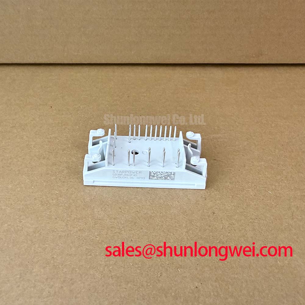
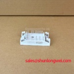
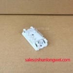
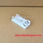
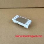
GD30PJX64F4S StarPower 600V IGBT Module for Industrial Inverters
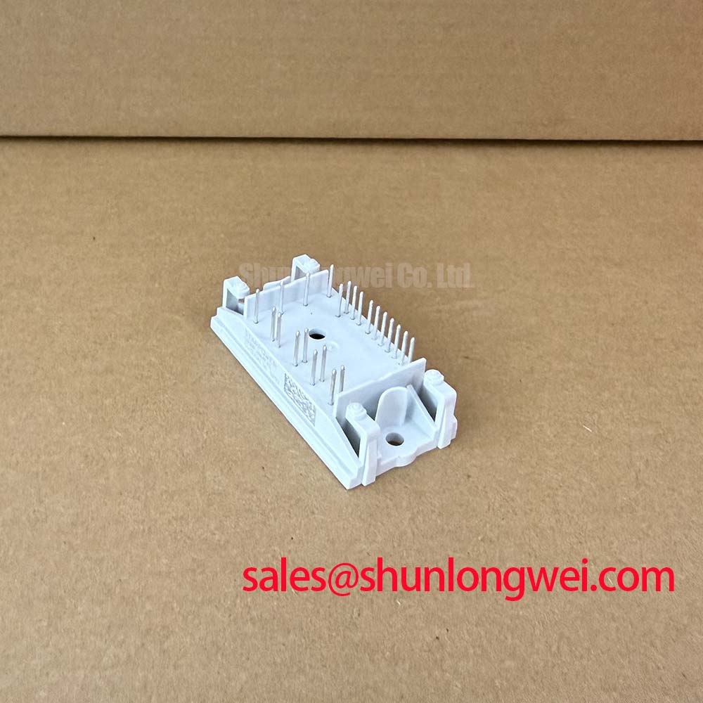
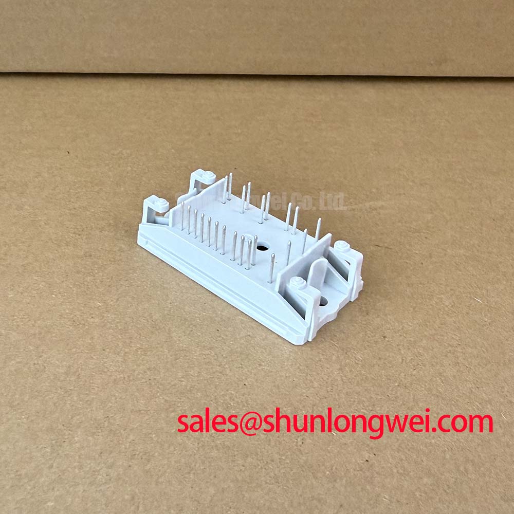
Begin a bench inspection by checking the part marking, examining the case and terminals for mechanical damage, and confirming the circuit’s rated boundaries before applying DC bus voltage. The GD30PJX64F4S is a StarPower IGBT module documented with a 600 V collector emitter voltage for the inverter IGBT, an 800 V repetitive peak reverse voltage for the rectifier diode, a 20 A continuous collector current for the brake chopper, and a 5.0 kΩ NTC resistance at 25°C.
These are official product specifications. They should be checked against the original inverter, drive, or high speed CNC spindle documentation before replacement. The available data identifies the principal functional blocks, but it does not establish every internal terminal assignment, switching waveform limit, isolation rating, gate drive requirement, or mechanical dimension. The system integrator should verify those items from the applicable manufacturer documentation and the equipment service manual.
| Functional Block | Parameter | Specification | Classification |
|---|---|---|---|
| Inverter IGBT | Collector emitter voltage, VCES | 600 V | Official Datasheet Specification |
| Rectifier diode | Repetitive peak reverse voltage, VRRM | 800 V | Official Datasheet Specification |
| Brake chopper | Continuous collector current, IC | 20 A | Official Datasheet Specification |
| Thermal sensor | NTC resistance at 25°C | 5.0 kΩ | Official Datasheet Specification |
Transient Dynamics and Electrical Design for the GD30PJX64F4S
During a field replacement, trace the power emitter return and the gate drive return separately before removing the original module. In a fast switching inverter, shared copper can allow load current changes to disturb the gate reference. That unwanted voltage is commonly treated as emitter mutual coupling. It can appear as ringing, uneven switching, or an apparently unstable gate signal even when the controller output looks correct at its connector.
Design Consideration: preserve a short, low impedance gate return path and keep the auxiliary emitter reference separate from the main high current emitter route wherever the confirmed terminal arrangement allows it. The gate loop, commutation loop, and DC link loop should be examined as distinct current paths. Designers should minimize the area enclosed by each high di/dt loop and avoid routing sensitive control traces parallel to the collector or brake switching path for extended distances.
Do not infer an unconfirmed Kelvin emitter connection from the package appearance alone. Verify the terminal definition from the original panel drawing or the applicable StarPower documentation. If the replacement board was modified in the field, photograph the conductor arrangement and compare it with a known good assembly before rework. A continuity check with the module fully isolated can identify an open connection or an unintended copper bridge, but a static test cannot confirm dynamic switching behavior.
For a compact industrial inverter or CNC spindle drive, inspect the gate waveform at the module reference point rather than only at the driver output. An oscilloscope comparison between the suspected phase and a known good phase can reveal common source inductance, connector contact problems, or an asymmetrical layout. The acceptable peak voltage and ringing envelope remain system determined and must be verified against the selected driver, insulation system, DC link, and switching conditions.
When the service stock requires a compatibility review, engineers may also evaluate GD15PJX120F4S as a separate StarPower device. It should not be treated as an automatic substitute. Voltage, current, pinout, thermal interface, gate charge, protection behavior, and mounting geometry must all be matched by the system designer.
Thermal and Electrical Optimization with an Isolated DC DC Supply
Check the isolated gate supply, its return path, and the driver reference before blaming the power module for irregular turn on behavior. The supplied product information confirms the inverter, rectifier, brake chopper, and NTC functions, but it does not specify a reinforced isolation voltage, common mode transient immunity, gate voltage range, or isolated DC DC power requirement for this exact device. Those values must be obtained from the relevant gate driver and module documentation rather than assumed from industry practice.
Engineering Recommendation: select the isolated supply only after accounting for gate charge, switching frequency, driver quiescent current, protection circuits, startup behavior, and the required isolation coordination. The isolation barrier should be assessed as part of the complete gate drive system, including creepage, clearance, transformer construction, PCB contamination conditions, and the actual common mode transient environment. A supply advertised for isolated gate drive use is not automatically suitable for every IGBT topology.
Keep the isolated supply loop physically close to the driver and use a controlled return path. The high frequency bypass network should be placed according to the driver manufacturer’s layout guidance. Excessive loop inductance can turn a normal gate current pulse into a voltage disturbance, while poor return routing can transfer collector transients into the control reference. The final layout should be validated with differential or suitably rated isolated probing during switching tests.
DC link stray inductance deserves the same practical attention. Place the local film suppression network close to the switching current path when the circuit design calls for it, and confirm its voltage, pulse current, dielectric, and temperature ratings. A snubber capacitor is not a universal cure for overshoot; its value, damping network, placement, and loss must be selected from measured waveforms. Designers should verify collector emitter peak voltage at the module terminals, not only at a remote DC bus test point.
The NTC provides a useful temperature feedback point during commissioning. At room temperature, the official reference value is 5.0 kΩ at 25°C. A resistance measurement that differs from the expected value should prompt inspection of the sensor wiring, connector contacts, temperature conditions, and the control board’s sensing circuit. It does not by itself prove that the IGBT silicon has failed. Record the temperature during measurement because NTC resistance changes with temperature.
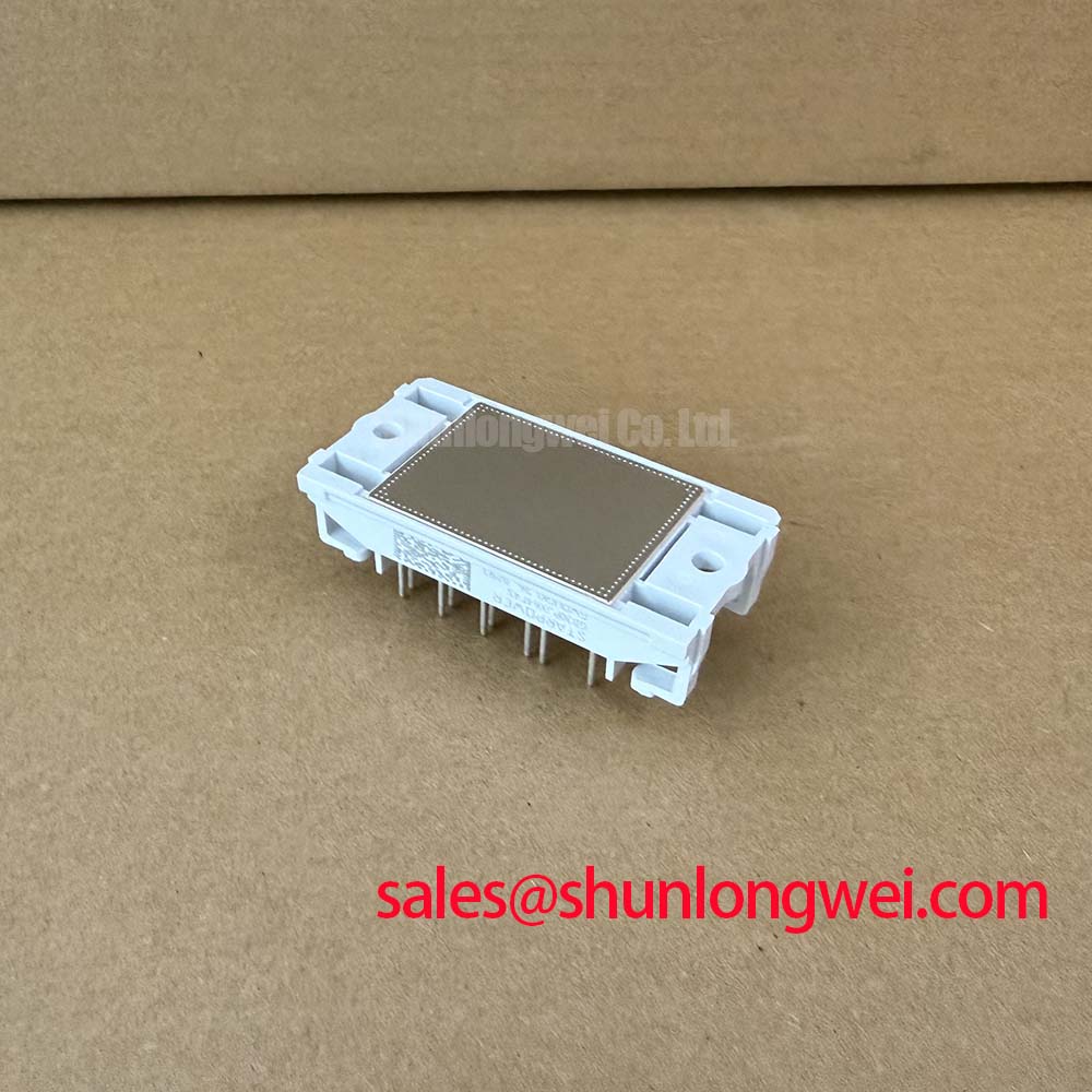
Thermal contact is equally important. Clean both mating surfaces, apply a uniform thin thermal interface layer suitable for the heatsink, and tighten fasteners according to the confirmed package and equipment service specification. Field Alert: never insert or remove the module wiring while the DC link or isolated gate supply can retain hazardous energy.
In the front end of a drive, the rectifier function should be reviewed together with the surrounding topology. The GD30PJX64F4S rectifier diode is specified at 800 V VRRM, but system commutation, reverse recovery, line conditions, and surge suppression determine the actual operating stress. Engineers reviewing a related front end may consult 5SNG015045P0301 as a separate peripheral topology reference, subject to independent electrical and mechanical verification.
Field Diagnostics and High Speed Desaturation Fault Management
Start a fault investigation with power removed and the DC link discharged according to the equipment procedure. Compare the suspected phase with an unused or known good phase using the same meter range and test conditions. Check for visible package cracking, loose bus connections, discoloration around the terminals, contamination near the gate circuit, and abnormal resistance between accessible power terminals. These checks are screening actions, not proof of a specific failure mode.
For a reported short circuit, inspect the gate driver supply, gate resistor network, desaturation or overcurrent signal path, and fault latch before installing another module. A low resistance reading can be influenced by parallel circuit paths, semiconductor junctions, snubbers, or measurement polarity. Isolate the relevant conductors where practical and compare the result with the equipment’s known good reference. Do not apply a high voltage insulation test to the module unless the manufacturer and equipment procedures explicitly permit it.
The supplied product information does not provide a confirmed desaturation response time, short circuit safe operating area, type I or type II protection timing, or a mandated soft turn off profile for this model. Those values must not be assigned by analogy. A gate driver may use staged fault handling in which the gate command is reduced before the device is fully turned off, but the correct sequence depends on driver architecture, gate impedance, DC link conditions, protection thresholds, and measured collector emitter behavior.
When commissioning a repaired drive, begin with a controlled low energy test and monitor gate emitter voltage, collector emitter voltage, phase current, fault feedback, and the NTC signal. Increase operating stress only after the protection path responds correctly under the equipment’s approved test method. The peak voltage margin is system determined. Verify it against the 600 V VCES rating and the complete switching transient, including busbar inductance, diode recovery, brake operation, and snubber behavior.
The rectifier diode’s 800 V VRRM rating should also be considered when examining line side surges or abnormal regeneration. Reverse recovery softness, EMI radiation, and commutation overshoot are properties of the complete diode, layout, load, gate timing, and suppression network. The available product data does not specify a softness factor or recovery waveform for the GD30PJX64F4S, so engineers should obtain those details from the applicable switching data and confirm them with controlled measurements.
The brake chopper specification gives a 20 A continuous collector current reference. This does not define the permitted pulse profile, duty cycle, resistor value, cooling requirement, or protection threshold. During a brake fault, check the braking resistor, wiring, command timing, DC link measurement, and thermal path as a complete circuit. A repeated chopper fault may involve system energy management rather than the module alone.
Circuit Protection and Reliability During High dv dt Operation
High dv dt switching can couple through gate collector capacitance and disturb an adjacent device’s gate reference. The practical response is to examine the gate waveform at the module terminals while the complementary switch changes state. Look for an unintended gate excursion, delayed turn off, asymmetric ringing, or a driver supply disturbance. If the control board signal is clean but the module terminal waveform is not, inspect the gate loop, return path, connector, and local decoupling before changing the controller.
Design Consideration: an active Miller clamp or another low impedance gate holding method may be appropriate when the selected driver supports it and the complete gate network has been validated. Negative gate bias is not an automatic requirement for this model. The supplied specifications do not state a negative gate voltage range, so any negative bias must be confirmed against the module and driver documentation, insulation coordination, gate oxide limits, startup sequence, and fault behavior.
Cross conduction should be evaluated through timing measurements rather than inferred from a single blown fuse or intermittent overcurrent alarm. Confirm dead time, driver propagation mismatch, gate resistor condition, supply stability, and the actual turn off and turn on waveforms for both complementary paths. The correct timing is system determined and must account for temperature, current, load power factor, driver delay, and the measured switching characteristics.
MOV protection can work with DC link clamps, RC or film suppression networks, and controlled switching, but the coordination must be calculated from the equipment’s surge energy and fault cases. The MOV voltage class, pulse energy, repetitive duty, thermal protection, and failure containment require system level verification. Do not treat an MOV as a substitute for short commutation loops or correct gate control.
Parallel semiconductor operation also requires measured static and dynamic current sharing. A positive temperature coefficient can support balancing under some operating conditions, but it does not guarantee equal current during turn on, turn off, short circuit, or uneven thermal contact. If multiple paths are used in the equipment, match the power loop geometry, gate drive timing, emitter reference, and heatsink interface, then verify sharing with current probes under the actual duty cycle.
Altitude and cosmic ray exposure may affect the voltage margin of power semiconductor systems, including single event burnout considerations, but no FIT value, SEB limit, altitude derating curve, or service life figure is provided for this product in the supplied specifications. These subjects require manufacturer data or a recognized reliability study. For general reliability terminology and the limits of statistical lifetime claims, engineers can review Mean Time Between Failures and Reliability Engineering. A related engineering discussion of wide bandgap switching constraints is available in Wide Bandgap Revolution.
For a compact inverter or high speed CNC spindle drive, final acceptance should combine the verified module ratings, confirmed terminal mapping, thermal interface inspection, gate waveform measurements, protection response, and the equipment manufacturer’s commissioning limits. The official ratings identify the electrical boundaries of the documented functional blocks; the surrounding drive determines whether those boundaries are respected during real switching events.