
Content last revised on September 25, 2026
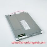
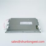
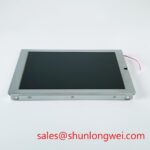
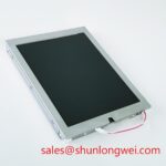
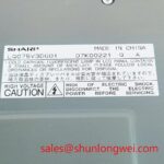
Sharp LQ075V3DG01 TFT LCD Display Module for Industrial HMI
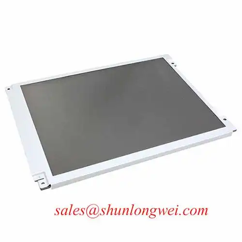
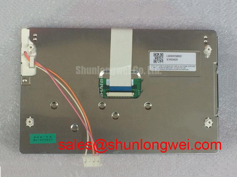
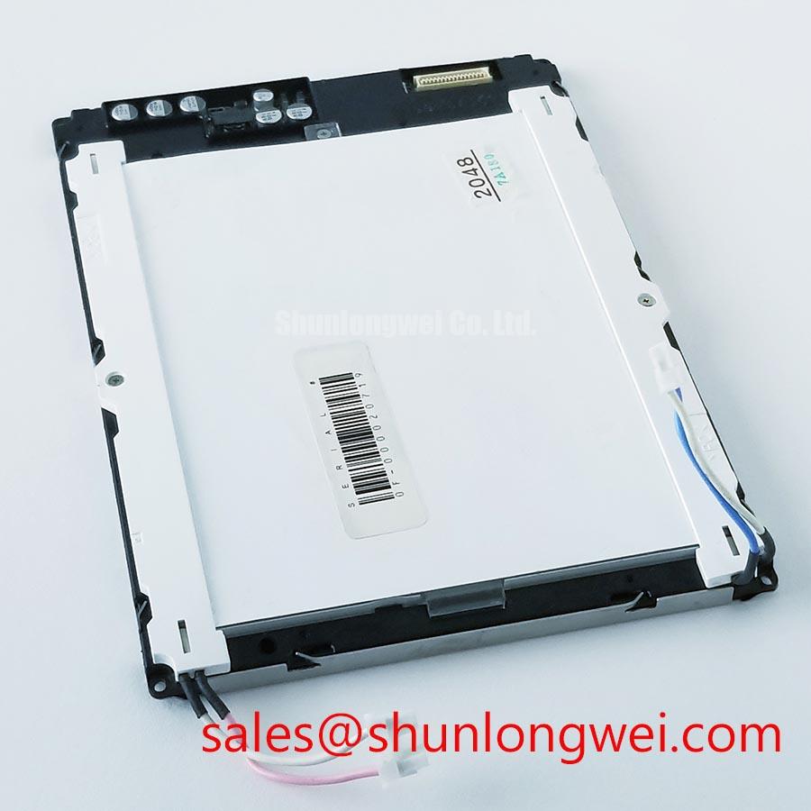
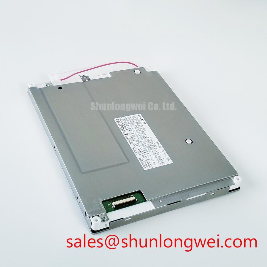
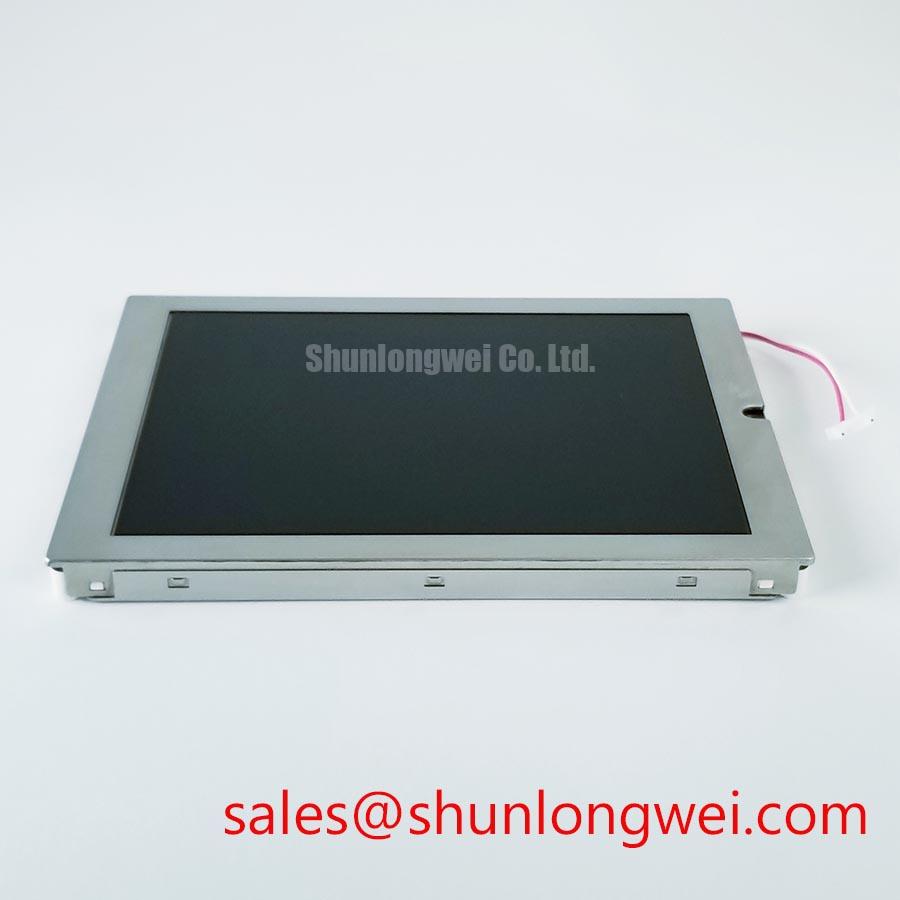
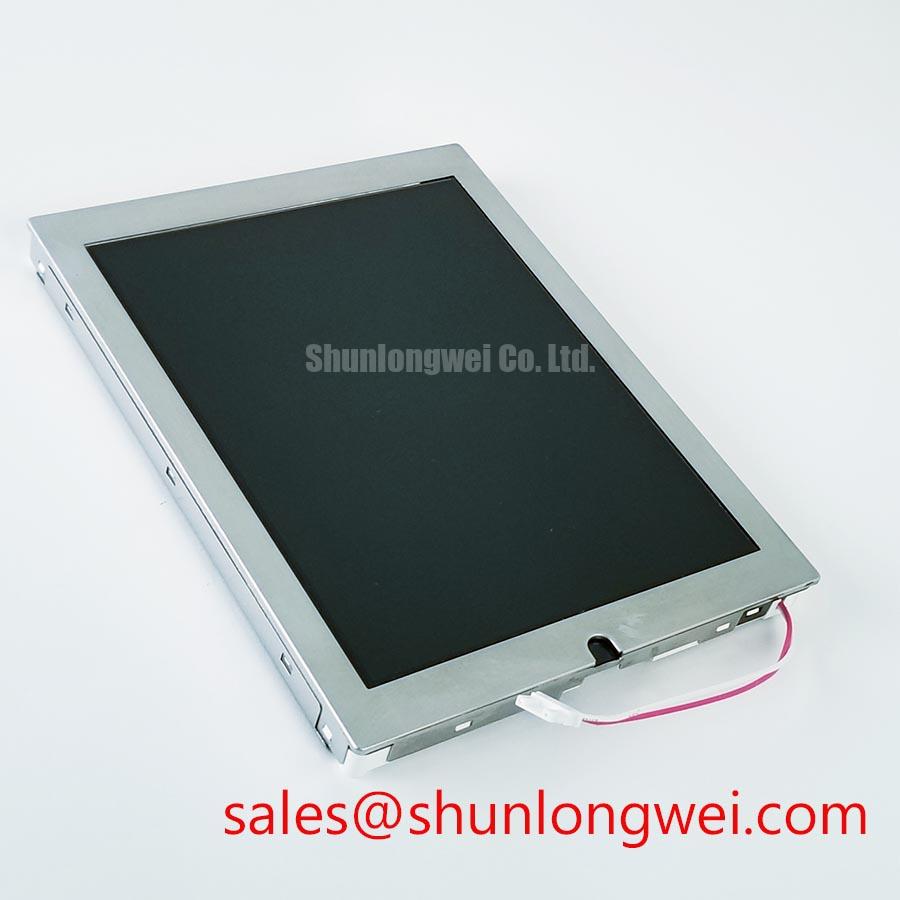
Measure the panel connector and inspect the bezel, mounting points, and display surface before applying power to a replacement LQ075V3DG01. This first check confirms that the incoming unit matches the original industrial display assembly and prevents an unknown interface or mechanical mismatch from being introduced into a live control console.
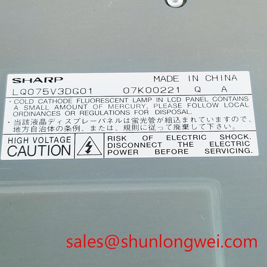
The Sharp LQ075V3DG01 is identified in the available factory information as an Industrial Grade LCD/HMI Panel supplied as a TFT-LCD Display Module. Its manufacturer is Sharp, and its specification status is recorded as Official Factory Spec Verified. The verified information supplied for this product does not establish a display resolution, interface pinout, supply voltage, backlight type, viewing angle, optical coating, or operating temperature range. Those values should be confirmed against the original panel documentation and the equipment service record before installation.
| Specification | Verified information |
|---|---|
| Model | LQ075V3DG01 |
| Manufacturer | Sharp |
| Product category | Industrial Grade LCD/HMI Panel |
| Construction classification | TFT-LCD Display Module |
| Specification status | Official Factory Spec Verified |
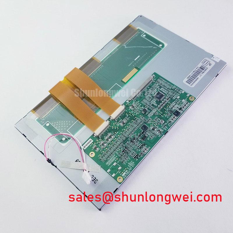
For a high-voltage substation protection or SCADA dispatch console, the display should be evaluated as part of the complete human-machine interface rather than as an isolated glass panel. The host controller, T-CON arrangement, backlight circuit, cable assembly, enclosure opening, and software timing all affect whether a replacement operates correctly. Where the original equipment documentation is unavailable, record the existing panel label, connector orientation, cable keying, backlight wiring, and controller board markings before disconnecting the old unit.
Thermal Expansion Clearance Sizing across Heavy Industrial Metal Enclosure Cutouts
Begin mechanical assessment by comparing the replacement panel’s visible display area, bezel envelope, mounting-hole pattern, connector clearance, and cable exit direction with the removed unit. The verified information for LQ075V3DG01 does not include dimensional drawings, so the outer envelope must not be inferred from the model number. Measure the enclosure cutout and the original panel directly, then compare those measurements with the supplier drawing or the manufacturer’s documentation before approving a mechanical fit.
In a metal industrial enclosure, the mounting frame and the display assembly can respond differently to temperature changes. This is a general Design Consideration, not a published LQ075V3DG01 factory limit. The panel should be supported evenly around its mounting area, with the enclosure opening free from burrs and the bezel free from concentrated pressure. A rigid bracket that contacts the visible display area can create mechanical stress, uneven brightness, or local optical non-uniformity. The system designer should determine the appropriate clearance from the enclosure material, panel dimensions, gasket construction, and expected temperature range.
Cross-pattern fastening is generally preferable to tightening one corner fully before the remaining points. If the original service documentation specifies fastener size and torque, follow that documentation. If it does not, the integrator should establish a controlled assembly procedure using a representative bracket and a torque verification test. The frequently used M3 range of 0.35 to 0.45 N·m may be treated only as a general industry design consideration for a suitable metal mounting arrangement, not as an official Sharp rating for this model.
Backlight behavior also needs to be traced to the original system. The supplied verified data does not identify whether this assembly uses a particular backlight technology, driver topology, dimming input, or brightness-control range. Do not connect a replacement driver based only on connector appearance. The system integrator should verify the backlight supply, current regulation method, enable signal, dimming polarity, and protection behavior from the original panel documentation and the host controller schematic. If PWM control is present, evaluate its frequency and duty-cycle response at the complete system level to check for visible flicker, acoustic interaction, or brightness non-linearity.
When a bezel or gasket is reused, inspect its compression marks and contact pattern. A gasket that has hardened or shifted can transfer enclosure stress into the panel during reassembly. The enclosure should also be checked for dust paths and moisture entry around the cutout. Optical bonding, sealing, and protective window arrangements are system construction features and should not be assumed from the LQ075V3DG01 model designation.
Backlight Inverter and Ignition Debugging
Before troubleshooting a dark display, separate the image-generation path from the backlight path. A panel may contain valid image data while the backlight remains inactive, and a bright backlight does not prove that the video interface is correctly configured. Inspect the original inverter or LED driver board, its connector labels, enable line, dimming line, and protective shutdown behavior. The available factory information does not confirm a dual-channel CCFL arrangement, a CCFL ignition voltage, an LED backlight, or a constant-current driver for this model.
For equipment that uses an external high-voltage CCFL inverter, ignition measurements must be performed with probes and procedures rated for the circuit. A commonly discussed cold-ignition range of 1500 to 1650 Vrms belongs to a possible inverter design consideration, not to the verified LQ075V3DG01 specification. The actual striking requirement depends on the lamp, tube condition, temperature, wiring, transformer, resonant network, and protection circuit. Engineers should confirm the original inverter documentation before interpreting a no-light condition.
For systems using an LED driver, measure the enable sequence and regulated output with suitable instrumentation while observing the host controller’s timing. A stated feature such as 1000:1 PWM dimming must come from the driver documentation; it should not be assigned to this Sharp panel without evidence. Audible noise, unstable brightness, or intermittent shutdown can involve the driver, cable routing, control waveform, thermal protection, or grounding arrangement. Compare the signal at the driver input with the known-good equipment waveform rather than assigning one symptom to one cause.
Video timing must be checked separately. The verified product information does not specify LVDS or TTL signaling, JEIDA or VESA mapping, clock frequency, data hold time, or transmitter jitter limits. The system integrator should verify the required interface from the original panel documentation. If the host uses LVDS, confirm the number of data lanes, pair order, polarity, termination arrangement, and mapping convention. If it uses a parallel TTL interface, confirm the pixel clock edge, data-bit order, synchronization signals, and enable timing before powering the display.
Temperature changes can alter the behavior of both the backlight circuit and the liquid-crystal response. A slow image response or visible contrast change at low temperature may involve the panel’s operating characteristics, controller settings, heater arrangement, or enclosure heat flow. The original operating-temperature specification should be obtained before qualifying the assembly for a cold environment. Long-life claims, half-life values, and MTBF figures should likewise be taken only from an applicable manufacturer document or independently controlled qualification report.
Controlled Differential Flex Routing to Suppress High-Frequency Jitter
Route the display cable only after identifying the actual interface used by the equipment. A model number alone does not establish whether LQ075V3DG01 accepts LVDS, TTL, or another signaling arrangement. Confirm connector pin names and voltage domains against the panel documentation, then inspect the host board for its serializer or timing-controller configuration. The system integrator should not apply a presumed 3.3 V or 5 V supply when the required voltage has not been documented.
For an LVDS implementation, the differential pairs should follow the impedance and length rules established by the transmitter, receiver, cable, and PCB stack-up documentation. A nominal 100 Ω differential impedance is a common high-speed design reference, but it is not a verified factory parameter for this model. The board designer must account for the actual dielectric structure, connector transition, flex geometry, return path, and termination scheme. Keeping each pair geometrically consistent is more useful than applying a nominal value without validating the complete interconnect.
Clock and data skew should be evaluated at the receiver under the real cable and temperature conditions. If split-screen artifacts, intermittent vertical bands, or unstable image content appear, inspect the complete signal path with a suitable oscilloscope and compare it with a known-good assembly. Possible contributors include pair polarity, mapping mismatch, insufficient return continuity, connector contamination, cable flexing, ground reference movement, or timing configuration. This method avoids treating a visible symptom as proof of a single failed component.
Power sequencing deserves the same attention. Confirm the order and timing relationship between logic supply, reset, display enable, backlight enable, and video data from the original controller documentation. The supplied verified information does not define a power-on rise-time window or a required delay for LQ075V3DG01. A white screen, residual image, or failed startup may involve the controller sequence, reset state, missing bias generation, backlight timing, or an incorrect interface mode. Capture the relevant rails and control signals during startup and shutdown before changing firmware or replacing the panel.
💡 Pro Tip: Keep each high-speed differential pair geometrically consistent through the flex, connector, and board transition, then validate clock and data timing on the assembled equipment rather than relying on a connector-level continuity check.
When assessing a possible replacement path, LM64P10 can be reviewed as a separate same-class display option, but compatibility must be established from physical dimensions, interface definition, timing, optical requirements, and backlight architecture. It should not be treated as an automatic substitute for LQ075V3DG01. In the power-tree review, LMS700KF01-001 may be examined as a related display solution or auxiliary-stage reference where its documented electrical role matches the equipment topology.
Surface Anti-Glare and Anti-Reflective Evaluation for High Ambient Readability
Evaluate the display in the actual enclosure with the intended protective window, bezel, ambient lighting, and operator viewing position. The available factory information does not confirm an AG coating, AR coating, IPS or MVA construction, TN characteristics, viewing-angle values, grayscale behavior, or optical bonding for LQ075V3DG01. These properties should be verified from the original Sharp documentation or a controlled sample inspection rather than inferred from the industrial LCD category.
High ambient light can reduce apparent contrast through reflections from the panel surface, front window, internal bezel, and nearby metalwork. A surface treatment may reduce reflected glare while changing haze, sharpness, or perceived black level. If a protective window is installed, assess its parallelism, surface finish, air gap, and reflection behavior with the complete display stack. An anti-glare result observed on an exposed panel may not remain the same after the unit is fitted behind a cabinet window.
Viewing-angle evaluation should use the actual interface settings and test images required by the application. Avoid assuming that a particular panel technology provides symmetrical viewing performance. TN, IPS, and MVA classifications have different optical behavior, but the technology used in this model is not established by the supplied verified parameters. Check grayscale transitions, dark-level uniformity, color shift, and text legibility from the operator’s normal position and from service-access angles.
For a protection or SCADA console, display readability is also affected by gamma configuration, T-CON bias settings, backlight regulation, and software color selection. The T-CON voltage rails and gamma references should be measured only against the applicable service documentation. If the panel remains functional but gray levels appear incorrect, verify the controller configuration and gamma data before concluding that the LCD cell is defective.
EMI testing should be performed on the complete display assembly, including the host controller, cable, enclosure, backlight driver, and grounding hardware. A differential pair target such as 100 Ω with a defined skew budget can be used only when it is supported by the interface design documentation and validated through measurement. LQ075V3DG01 itself should not be described as independently certified for system-level EMC compliance. For broader display interface, optical, and integration considerations, consult The Ultimate Guide to Industrial TFT LCD Technology alongside the original equipment documentation.