Content last revised on September 14, 2026
M505013F Circuit Protection & Reliability: Calibrating Non-Repetitive Surge On-State Current
In a grid-tied Static Var Compensator or thyristor-switched capacitor cabinet, the device is exposed to switching events that are different from its normal periodic load current. A technician should therefore separate the continuous current check from the non-repetitive surge assessment. The 50.0 A rated current is an official product-record value, but it should not be treated as the permissible value for every capacitor energization event, fault transient, or 10 ms half-cycle surge.
The relevant factory parameter is the non-repetitive surge on-state current, commonly identified as ITSM for a sinusoidal half-cycle condition. No ITSM value is included in the supplied parameter set, so the repair engineer should obtain the correct data sheet revision and verify the test waveform, initial junction temperature, pulse duration, and repetition conditions. A surge rating is meaningful only when the actual SVC switching sequence matches the manufacturer’s stated conditions. Reapplying reverse voltage before the junction has returned to a safe thermal state can produce a different stress profile from the original surge test.
Fuse coordination requires the manufacturer’s specified I2t relationship rather than a generic fuse selection. Compare the prospective capacitor-switching current, fuse clearing behavior, and the module’s published surge withstand information as one protection set. If the original fuse is unavailable, the system designer should recalculate the coordination from the verified semiconductor and fuse data. A fuse with a suitable nominal current may still provide unsuitable let-through energy during a high-current transient.
Terminal inspection should include conductor condition, lug seating, oxide contamination, and evidence of localized heating. Measure the complete power path with the equipment isolated and discharged, then compare each phase or branch with a known-good path where the cabinet design permits. A low-resistance reading alone does not confirm dynamic thyristor health, because junction leakage, gate sensitivity, commutation behavior, and thermal performance require additional tests.
Mechanical installation is part of the protection system. Confirm that the mounting surface is clean, flat, and free from burrs before applying the module’s specified interface material. The exact mounting torque, terminal torque, washer arrangement, and tightening sequence must come from the applicable SanRex or Crydom mechanical drawing. Do not substitute a general torque value for a factory instruction, since excessive pressure can distort an isolated package while insufficient pressure can increase thermal impedance.
💡 Pro Tip: Isolate and discharge the cabinet before removing any power or gate connection, then document terminal orientation and conductor routing before disturbing the original assembly.
M505013F Thermal-Electrical Optimization: Gate Trigger Current and Temperature-Dependent Practical Tuning
Gate control should be verified as a complete circuit rather than judged only by the presence of a trigger pulse. The manufacturer’s data should be consulted for IGT, VGT, gate reverse limits, pulse duration, and allowable peak gate current. Those values are not present in the supplied product record and must not be inferred from the 50.0 A load-current rating.
For an SVC or thyristor-switched capacitor branch, inspect the trigger transformer or isolated driver, gate wiring, return path, connector condition, and synchronization logic. The gate pulse should be observed at the module terminals with an oscilloscope and an appropriate isolated measurement arrangement. A pulse measured at the driver output may not represent the pulse reaching the gate after wiring impedance, common-mode movement, and connector voltage drop are included.
A fast gate-current rise is often discussed in thyristor firing design, but the correct target depends on the device data sheet and the firing circuit. If a design requires a gate-current slew condition such as dIG/dt greater than 1 A/µs, that value must be treated as an application requirement to verify, not as an official M505013F rating. Engineers should confirm the actual triggering requirement with the manufacturer’s specified test circuit before modifying the pulse network.
Temperature can change the practical firing margin. During a controlled test, record the module case temperature, supply synchronization, gate pulse amplitude, gate pulse width, and load condition. A trigger circuit that operates correctly when cold may behave differently after the heatsink and cabinet have reached operating temperature. This observation does not identify one universal fault cause; it indicates that the gate and thermal conditions should be measured together.
Back-porch current or sustaining gate current may be used in a multi-pulse firing scheme, but its value and timing must be established from the factory gate characteristics and the system controller’s isolation design. Repeated pulses should not be added solely to compensate for an unknown wiring problem. Excessive gate drive can raise local dissipation, while insufficient pulse energy can create inconsistent latching under the actual anode current waveform.
Gate-loop layout deserves particular attention in high-power switching cabinets. Minimize the area of the gate and return loop, keep it separated from high di/dt power conductors, and evaluate the driver reference against common-mode ground movement. Negative turn-off bias, if used by the system, must remain within the device’s verified gate reverse-voltage boundary. The appropriate bias value, damping network, and pulse timing are system-determined and should be validated during switching tests rather than imposed as fixed values for this part.
Transient Dynamics & Electrical Design: Reverse Recovery Charge on M505013F
Before using this module in a topology that includes antiparallel or commutating semiconductor paths, establish the internal configuration from the correct product drawing. The supplied product information confirms the M505013F category and ratings, but it does not provide a diode reverse-recovery charge, peak reverse-recovery current, recovery time, or softness classification. These parameters must be verified directly from the relevant manufacturer documentation.
In a capacitor-switched SVC branch, commutation behavior depends on the capacitor voltage, reactor or line impedance, firing angle, current direction, stray inductance, and the recovery characteristics of the semiconductor path. A replacement evaluation should therefore use the actual cabinet topology. Monitor voltage across the module and current through the branch during controlled switching tests, and compare the waveforms with a known-good assembly or the original design record.
When the applicable data sheet provides IRRM and trr, compare those values with the system’s measured commutation waveform. Reverse-recovery charge can increase current stress in the opposing path and can intensify voltage overshoot through unavoidable loop inductance. The engineering objective is to minimize the commutation loop and verify peak voltage margins against the 2500.0 V rated voltage under the real switching condition. The voltage rating is an official product-record value; it is not a blanket approval for every repetitive transient.
EMI evaluation should be performed at equipment level. Probe placement, current return paths, cabinet bonding, busbar symmetry, snubber condition, and control-cable routing can all affect the measured result. The semiconductor module itself should not be described as independently certified to an equipment EMC standard. If the cabinet is evaluated against an applicable emissions requirement, the complete SVC assembly and its installation environment must be tested.
For current measurement, select a sensor with adequate bandwidth and insulation for the test arrangement. Engineers may evaluate Hall, fluxgate, GMR, or TMR approaches according to the required bandwidth and isolation. Background on GMR sensing is available in this GMR and TMR sensor reference. For heating analysis, use the measured RMS current and the actual conduction path rather than assuming that the nameplate current represents the cabinet’s thermal load. The general RMS concept is described in this RMS current reference.
A preceding rectifier or protection stage may determine the voltage and current waveform presented to the switching module. In a system-level review, the related PD25016A can be examined as a neutral reference for a possible upstream or complementary topology element, subject to confirmation of the original circuit documentation. This is not a substitute recommendation for M505013F; electrical function, pin arrangement, voltage class, current behavior, and mechanical compatibility must be checked independently.
M505013F Circuit Protection & Reliability: Calibrating Baseplate Thermal Resistance
Thermal verification begins with the mechanical interface. Confirm that the heatsink or clamping structure is clean, level, and free of particles that could create a local pressure point. The supplied package description is Isolated Power Module, but the supplied factory data does not include Rth(j-c), baseplate dimensions, contact pressure, or an approved mounting torque. These values should be taken from the exact mechanical and thermal documentation for the unit being installed.
Where a flat clamped interface is used, apply the specified thermal interface material evenly and avoid excess compound migrating toward terminals or insulation surfaces. If the assembly uses a pressure plate or disc-spring arrangement, calibrate the pressure according to the equipment drawing and inspect the spring stack for correct order, seating, and condition. Tightening one side fully before the opposite side can create an uneven contact pattern and can distort the module or heatsink.
During a thermal test, log case temperature at defined load conditions while also recording ambient temperature, airflow, heatsink condition, switching state, and current waveform. A stable case reading does not by itself prove that the junction is within its permitted operating range. The engineer must combine the measured case condition with the manufacturer’s junction-temperature limit, transient thermal data, and the actual power dissipation derived from the operating waveform.
Conduction loss assessment should use the manufacturer’s on-state characteristic at the relevant junction temperature and current. Do not calculate dissipation from the 50.0 A rated current alone. RMS current, duty cycle, firing angle, crest factor, and commutation intervals can materially change the thermal result. If the cabinet operates with repeated capacitor energization, include the transient sequence in the thermal profile rather than validating only the steady-state condition.
Uneven heating across the baseplate may justify an inspection of heatsink flatness, fastener sequence, interface coverage, busbar stress, or airflow distribution. It should not be assigned to one cause without measurement. Infrared inspection can assist with comparative checks, but emissivity, reflective surfaces, and access limitations should be controlled. Thermocouple placement and electrical isolation should follow the test plan used for the cabinet.
When comparing the M505013F with another device, compare the complete application boundary instead of relying on a single voltage or current figure. The PK55FG120 may be reviewed as a separate option in a cross-reference exercise, but its topology, ratings, gate behavior, thermal interface, and mechanical outline require independent confirmation before any substitution decision. The broader Power Semiconductor Selection Guide provides a useful framework for reviewing electrical, thermal, protection, and integration conditions together.
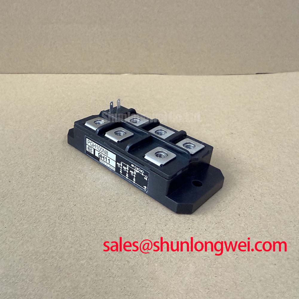
For procurement and service records, retain the exact manufacturer marking, electrical rating confirmation, package description, application circuit, terminal map, approved heatsink method, and test results. The verified product-record identity for this page remains M505013F from SanRex / Crydom, with 2500.0 V, 50.0 A, and an Isolated Power Module package as the supplied official specification set.