





Content last revised on September 28, 2026
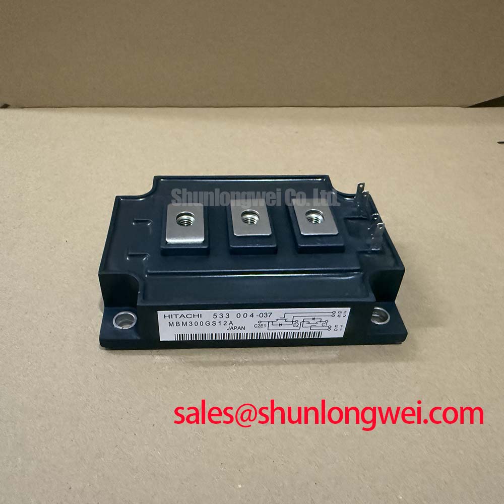
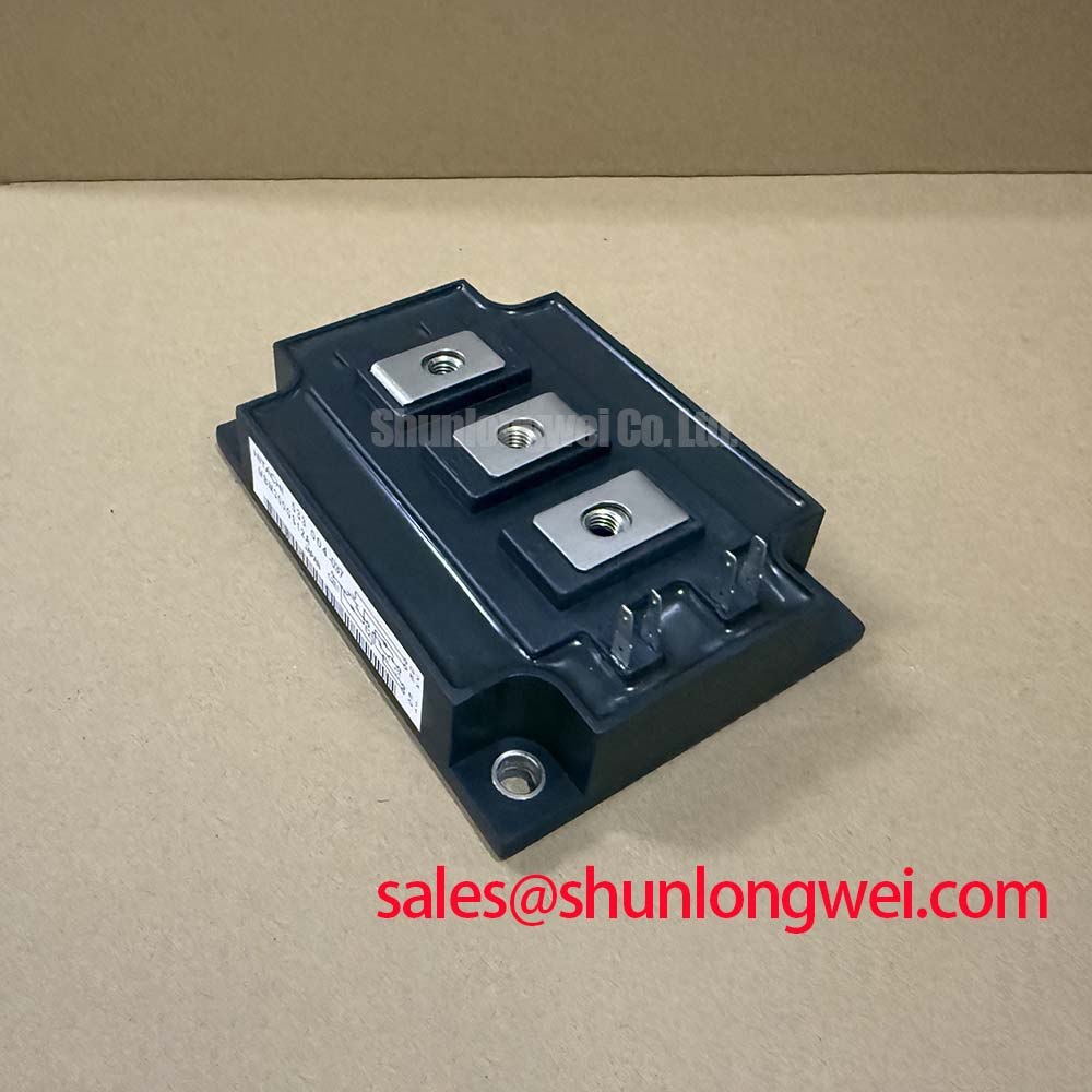
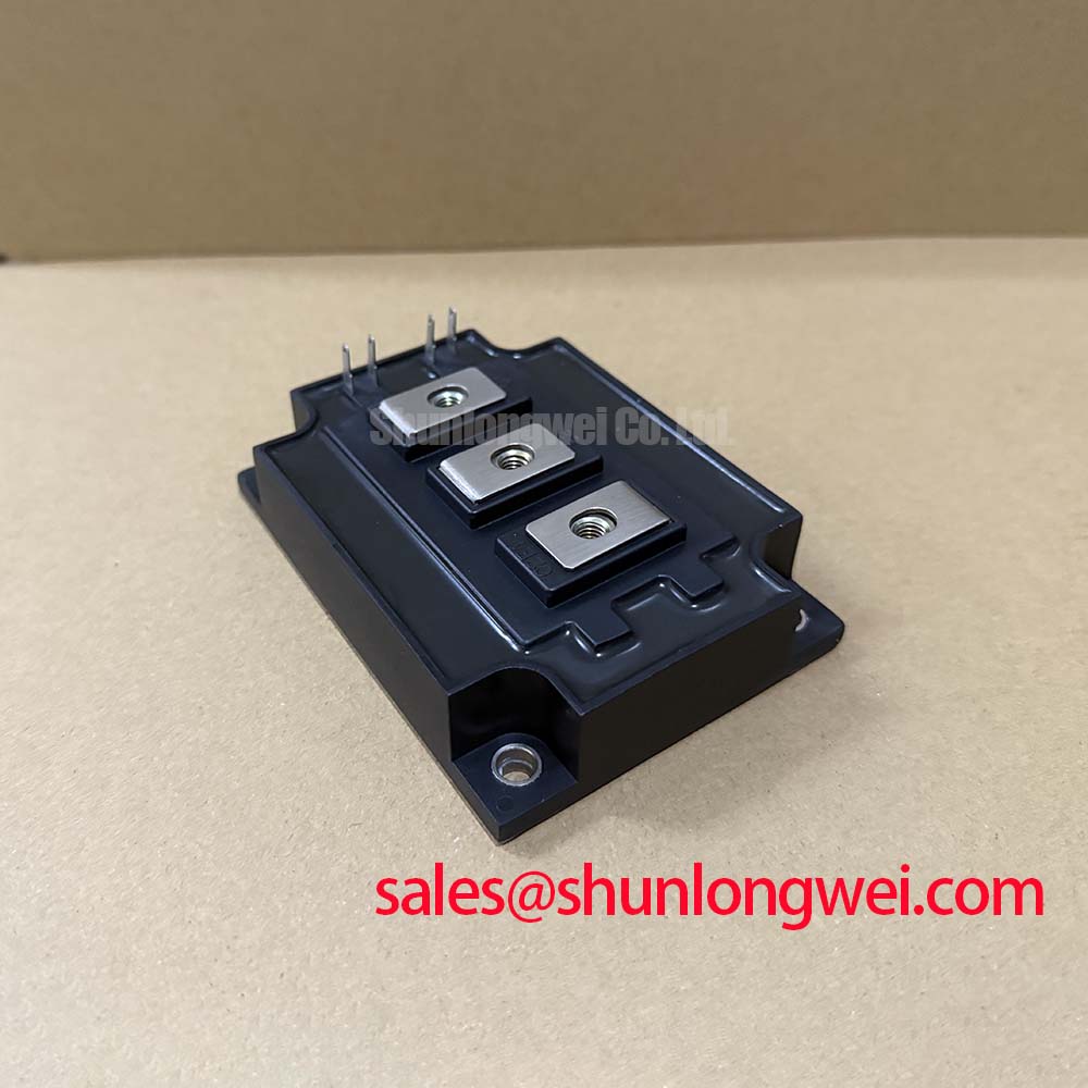
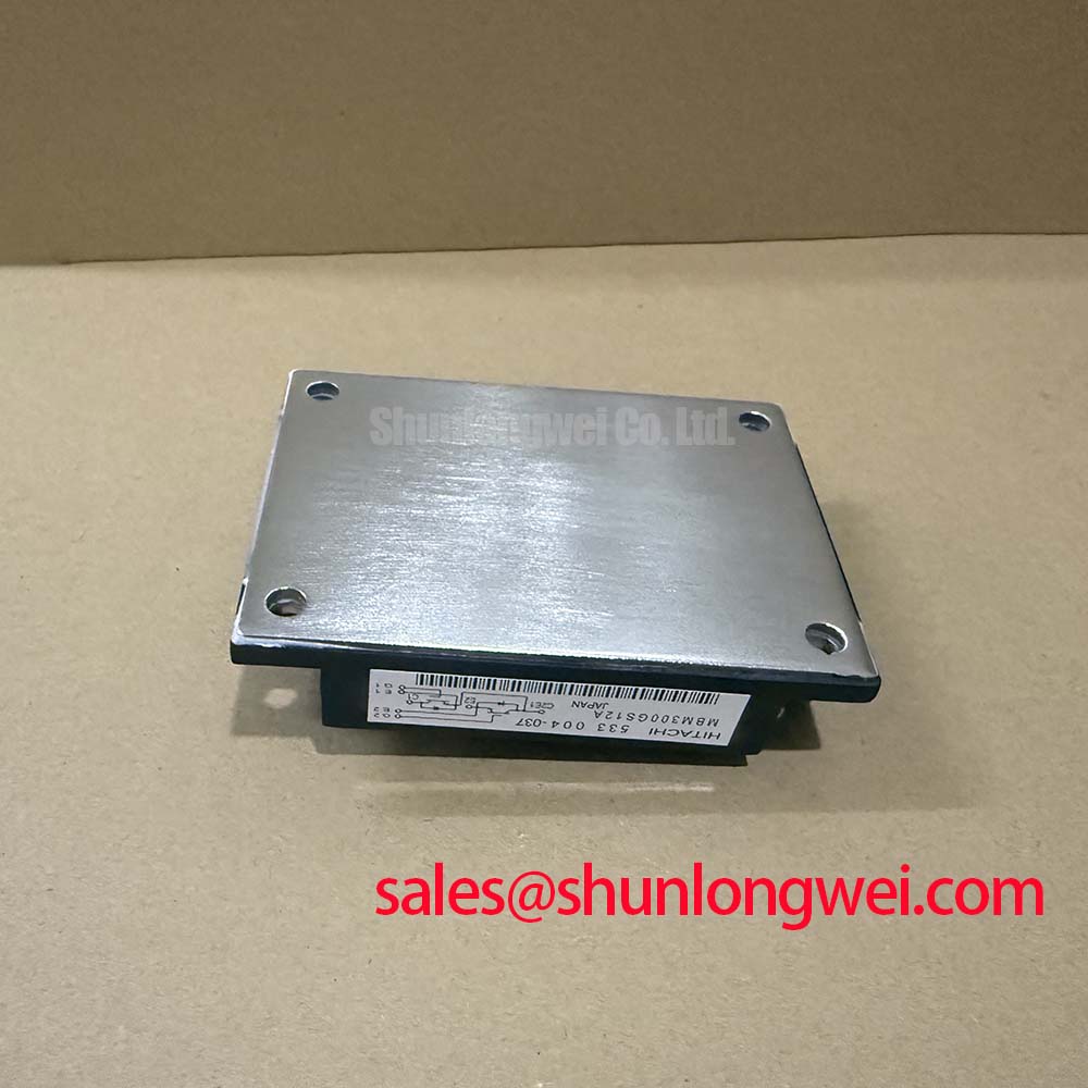
MBM300GS12A Thermal-Electrical Optimization: Symmetrical Busbar Geometry for High-Current Practical Tuning
The official switching specification lists a typical total switching energy of Ets = 28 mJ at IC = 300 A and Tj = 125°C. This value should be treated as a device specification under its stated test conditions, not as a complete system loss calculation. Actual inverter dissipation also depends on switching frequency, gate-drive timing, junction temperature, current waveform, and the external commutation path.
Design Consideration: Keep the high-current DC bus geometry physically symmetrical so that parallel current paths do not introduce avoidable impedance differences. During commissioning, compare phase-leg voltage waveforms and terminal temperature rise under controlled load. Uneven heating may justify checking busbar contact pressure, surface condition, torque verification, and the thermal interface rather than assuming an internal module fault.
For phase-controlled rectifier sections, the conduction angle and line impedance affect harmonic current. The system designer should evaluate the measured line current with the selected rectifier and filtering arrangement, then verify compliance at the complete drive input. The MBM300GS12A itself should not be described as independently providing grid harmonic compliance.
In regenerative braking circuits, the chopper path and braking resistor absorb energy generated by the motor and DC link. Confirm that the drive control system limits DC-link rise within the verified switching and voltage boundaries. The module rating alone does not determine resistor thermal capacity, braking duty cycle, or system protection settings.
Transient Dynamics & Electrical Design: Turn-Off di/dt Induced Vpeak Clamping on MBM300GS12A
During turn-off, stray inductance in the commutation loop converts rapid current change into an overvoltage across the switching path. In engineering terms, the peak voltage rises with DC-link voltage, loop inductance, and current slew rate. Minimize the high-current loop area, maintain symmetrical planar busbar routing, and verify the resulting peak with a properly connected oscilloscope probe during switching tests.
Snubber selection is system-dependent. Designers should assess capacitor pulse current, voltage rating, damping behavior, physical placement, and the measured ringing frequency rather than applying a universal capacitance value. Gate-drive source and sink capability should also be checked against the selected gate resistance and the required switching profile. External damping resistance is a tuning element; the correct value must be established from waveform measurements, switching loss, and thermal results.
The 28 mJ typical total switching energy is useful when comparing controlled test conditions, but it does not replace a complete loss model for a variable frequency drive. A service engineer should record DC-link voltage, load current, switching temperature, and turn-off waveform together when investigating unexplained heating.
High-speed semiconductor protection remains part of the surrounding power architecture. The Mersen Protistor® High Speed Semiconductor Protection Fuses resource provides industry information for evaluating semiconductor fuse protection; fuse coordination must still be verified against the actual drive topology and fault energy.
MBM300GS12A Operational Boundaries: Evaluating Active Miller Clamp Implementation Limits
High dv/dt can couple through the power device capacitances and disturb the opposite switch gate. An active Miller clamp may help hold the inactive gate at a controlled low impedance, but compatibility depends on the isolated driver, gate loop layout, propagation delay, common-mode behavior, and the module’s documented gate requirements. The system integrator should verify the required gate voltage range and any negative-bias arrangement from the original drive documentation rather than assuming a fixed value.
Keep the gate-drive return separate from noisy power-current paths wherever the module interface permits it. If a dedicated emitter-return or auxiliary gate reference is present in the original assembly, preserve that routing concept and validate it with differential probing. A gate waveform that differs substantially between the upper and lower devices may indicate layout coupling, driver imbalance, or measurement error; compare it with a known-good phase leg before replacing hardware.
At the thermal interface, clean both mating surfaces, inspect the heatsink flatness, and apply the approved thermal interface material according to the equipment service specification. Cooling performance should be confirmed by checking contact temperature, airflow, and the condition of the heatsink rather than by relying only on the module’s current rating.
Maintenance Note: Record heatsink temperature rise during scheduled service and recheck airflow and terminal tightness after dust removal or thermal-interface work.
Field Diagnostics & Commissioning: Mitigating Hard-Switching Transients in MBM300GS12A Topologies
Commissioning should begin with the drive isolated and discharged, followed by visual inspection, continuity checks appropriate to the circuit, and confirmation that the gate driver is referenced correctly. Do not infer a semiconductor failure from one resistance reading; compare all equivalent phase paths and review the result alongside gate signals, DC-link behavior, and load conditions.
Short-circuit protection requires a fast detection path, controlled fault response, and a turn-off strategy that limits additional inductive overvoltage. Type-I and Type-II protection behavior, desaturation sensing, blanking time, and soft turn-off timing must be verified from the driver and system design documentation. The MBM300GS12A rating does not by itself establish a guaranteed short-circuit withstand interval.
For a replacement assessment, compare mechanical mounting, electrical ratings, terminal arrangement, gate-drive requirements, and cooling conditions against the original equipment documentation. A related device such as MBM200JS12EW should be evaluated only as a separate compatibility case, not assumed to be a drop-in substitute. For longer-life switching evaluations, the technical discussion in The 1200 V CoolSiC™ MOSFET Advantage in Three can provide broader context, while final validation remains dependent on the actual drive topology, thermal path, and measured switching margins.