



Content last revised on September 28, 2026
MBN1200D33A Benchtop Checks and Switching Voltage Stress
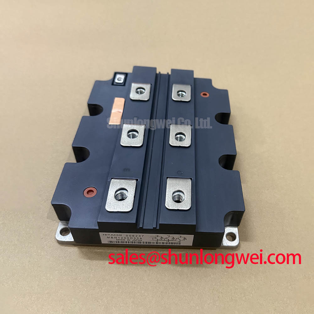
With the equipment isolated and its DC link discharged, check the MBN1200D33A terminal markings against the original Hitachi connection drawing before placing a meter across any power terminals. Record cold-state gate-to-emitter resistance and diode-mode readings, then compare them with a known-good unit tested at a similar temperature. A diode-mode reading can help establish polarity and identify an obvious short, but it cannot verify high-current switching performance.
💡 Bench Tip: Keep the gate and emitter protected from electrostatic discharge during incoming inspection, and record the meter lead polarity alongside each diode-mode result.
The supplied official specifications rate collector-to-emitter voltage at 3300 V and continuous collector current at 1200 A with case temperature at 80 °C. Gate-to-emitter voltage is rated at ±20 V. These are device boundaries, not a prescribed DC-link setting or gate-drive waveform. As a Design Consideration, capture collector-to-emitter voltage at turn-off under the intended load and compare its peak with the rated limit. Layout, busbar inductance, gate control and operating conditions determine the observed overshoot.
Altitude and terrestrial radiation can enter a high-voltage system reliability review, but no device-specific single-event burnout rate, voltage-derating curve or failure-in-time figure is provided here. A numerical prediction for this module would require applicable manufacturer data and operating conditions. For a commercial string inverter or microgrid energy-storage converter, the system engineer should establish voltage headroom from measured switching stress and the project’s reliability criteria rather than treating the nameplate voltage as a recommended operating point.
Field Diagnostics: Gate Drive and Insulation Boundaries
Before commissioning, trace each gate-drive connection from the driver board to the module terminals using the original connection drawing. Confirm the return path actually used by the installed driver; do not assume this module has a separate Kelvin-emitter terminal without a verified pinout. If a separate sense return is documented, routing it away from the high-current emitter path is a Design Consideration for reducing shared-inductance disturbance. Compare gate-to-emitter waveforms at the module during switching, especially when the complementary device changes state.
The ±20 V gate-to-emitter rating is an Official Specification and applies to the voltage seen at the module terminals, including transients. Unexpected gate pulses call for waveform checks of driver supply stability, return-path coupling and switching-node behavior. The driver’s common-mode transient immunity belongs to the selected driver and its implementation; a specific immunity rating cannot be assigned to the MBN1200D33A from the supplied module data.
⚠️ Field Alert: Never perform resistance or diode-mode checks while the DC link remains energized or charged.
Likewise, do not infer a reinforced-isolation withstand rating for the module from its collector-to-emitter voltage rating. Verify barrier requirements, creepage, clearance and the appropriate test procedure against the complete assembly documentation before applying an insulation test. Where a high-side driver uses a bootstrap supply, its capacitor must support gate charge and driver consumption throughout the intended switching and idle intervals. Those inputs require driver and module charge data that are not supplied here; capacitor sizing remains a system-design calculation.
Bidirectional Converter Checks Without Assuming Topology
A bidirectional battery-to-DC-link converter can be evaluated as a potential integration context for the MBN1200D33A, not as a confirmed intended application. In either power-flow direction, inspect the actual circuit diagram to identify which switch conducts, which path carries freewheel current and how the controller limits current during a change of operating mode. The official continuous-current rating of 1200 A at 80 °C case temperature does not establish allowable current for every duty cycle or cooling arrangement.
When a freewheel diode commutates, reverse-recovery behavior can affect voltage overshoot and radiated noise. Recovery softness is an application-relevant Design Consideration, but no softness factor or recovery waveform is included in the supplied specifications. Compare switching-node voltage and current waveforms under representative conditions rather than assigning the module an undocumented recovery characteristic. For a detailed discussion of different semiconductor approaches, the Wide Bandgap Revolution guide provides broader technology context; it does not establish this Hitachi module’s diode behavior.
For a maintenance substitution review, MBM200H45E2-H can be examined as a separate candidate only after its voltage and current ratings, terminal arrangement, dimensions, gate requirements and thermal characteristics have been checked against the equipment documentation. A model reference alone is not evidence of interchangeability. If gate leakage or insulation readings raise questions during incoming QA, repeat the test under the documented method before interpreting the result. Quantum tunnelling describes a general physical phenomenon; it is not a basis for diagnosing this module’s gate structure from a handheld-meter reading.
MBN1200D33A Thermal Limits Under Pulsed Operation
The supplied official specifications give typical collector-to-emitter saturation voltage as 3.5 V at 1200 A, total power dissipation as 8.9 kW at 25 °C case temperature, and operating junction temperature as −40 to +125 °C. Keep the stated conditions attached to each figure: a typical saturation value is not a worst-case loss guarantee, and a power-dissipation rating at one case temperature does not describe a converter’s continuous cooling capacity.
For pulsed overload evaluation, record current, conduction interval, switching activity and case temperature at the module mounting location. Transient junction rise depends on the time-varying losses and the module’s transient thermal impedance. A multi-RC thermal model can be used as an Engineering Calculation only when its parameters come from applicable manufacturer thermal data; none are supplied here. Without those parameters, a numerical peak-junction-temperature margin would be speculative.
Inspect mounting contact and cooling performance if case temperature rises unexpectedly, while checking electrical losses at the same operating point. Repeated temperature swings matter to a Design Consideration of thermal cycling, but no cycle-life prediction is supported by the supplied specifications. Complete the assessment by comparing measured case temperature and calculated junction behavior, where validated thermal data exist, with the specified +125 °C junction limit.