Content last revised on September 15, 2026
Thermal and Surge Margins During High-Peak Events for MD165C16D2
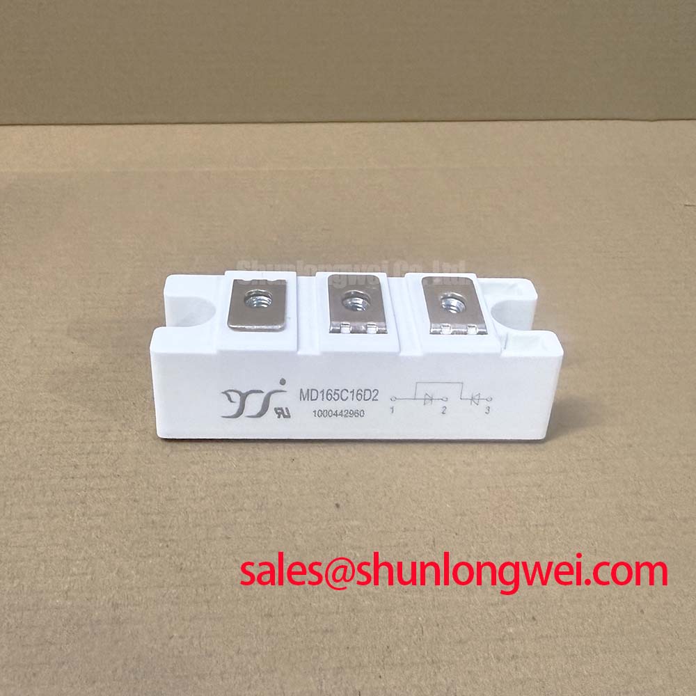
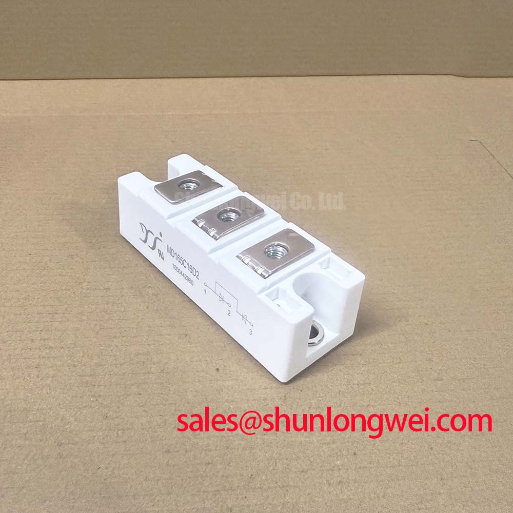
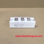
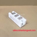
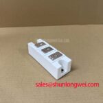
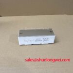
With the module isolated from the equipment, first trace each power terminal against the host connection diagram and compare diode mode readings across the expected current paths before applying any voltage. The MD165C16D2 from SanRex (Sansha Electric) is a three phase bridge diode module rated at VRRM 1600 V and ID 165 A at TC 100°C, according to the official factory specification. Its specified maximum forward voltage drop is 1.35 V at 165 A, while the specified AC isolation breakdown voltage is 2500 V for 1 minute.
For incoming inspection, a diode mode check can identify an unexpected short or open current path, but it does not replace a controlled high voltage isolation test or a loaded thermal assessment. The module is specified with IFSM 1500 A for one 60 Hz cycle and Rth(j c) 0.16°C/W. These ratings define essential device boundaries, yet the original equipment circuit, heatsink interface, fuse coordination, busbar geometry, and cooling condition remain system dependent.
The official surge value for MD165C16D2 is 1500 A for one 60 Hz cycle. It should not be relabeled as a 10 ms half cycle rating because the stated factory condition is one full 60 Hz cycle. A repair engineer assessing a current event should therefore document the actual waveform duration, repetition rate, initial case temperature, and phase location rather than treating the surge figure as a continuously usable overload current.
This is a diode bridge module, not a controlled thyristor bridge. There is no gate circuit, firing angle, latching behavior, or avalanche rating provided in the listed factory parameters. Design Consideration: repeated fault pulses can accumulate junction heating even where each individual pulse appears lower than the published single cycle surge condition. Confirm that reverse voltage is reapplied only after the affected circuit has returned to its intended electrical state and that the measured transient voltage stays within the 1600 V repetitive peak reverse voltage rating.
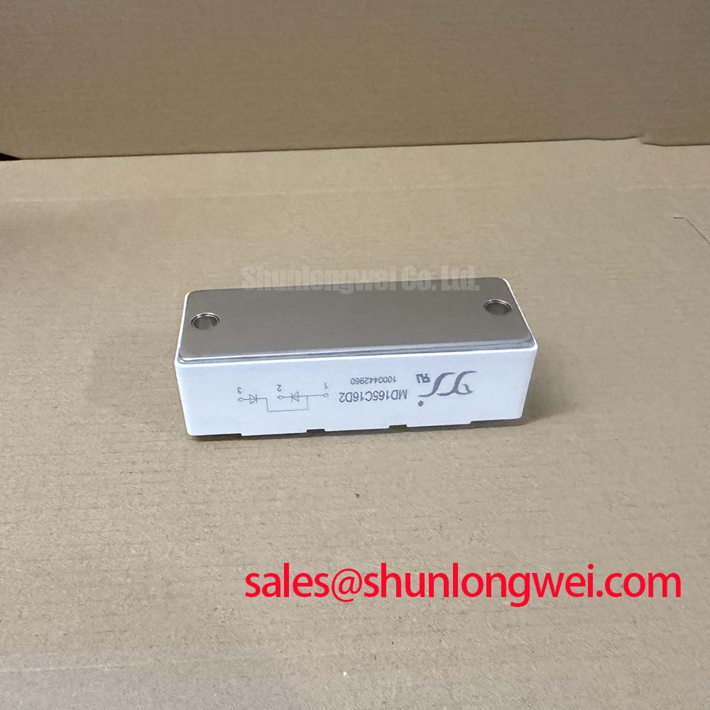
Before returning a rectifier cabinet to service, inspect the mating heat spreader for flatness, contamination, and uneven contact marks. The specified 0.16°C/W junction to case thermal resistance describes the semiconductor to case path only; it does not include thermal interface material, heatsink resistance, airflow, coolant performance, or cabinet temperature. The mounting hardware size and torque are not included in the supplied factory data, so the installer should use the equipment maker’s mounting instruction and the module documentation rather than applying a generic torque value.
💡 Bench Tip: Disconnect stored energy sources and establish cold state diode mode readings before comparing a suspect bridge module with the known circuit path.
Where a higher current three phase bridge is being assessed during an equipment redesign, FRS200CA100 can be reviewed as a separate reference part, with terminal arrangement, thermal path, voltage class, and protection requirements verified independently.
Transient Dynamics & Electrical Design: Power Factor Degradation and Harmonic Mitigation on MD165C16D2
MD165C16D2 performs diode rectification, so firing angle control from 0 to 150 degrees is not a function of this module. If an upstream controlled rectifier, transformer tap changer, or active front end establishes DC output regulation, its firing sequence and power factor behavior belong to that system stage. The diode bridge should instead be evaluated for its actual phase current waveform, reverse voltage exposure, commutation conditions, and heat rejection at the documented operating point.
Design Consideration: line current distortion and reactive power can change when a DC load becomes discontinuous, when source impedance rises, or when a controlled upstream stage changes conduction timing. Engineers should measure phase voltage and current together at the equipment input, then compare the result with the original commissioning limits. This avoids assigning harmonic symptoms to the diode module without evidence from the power path.
For a high current green hydrogen electrolyzer DC power rectifier, the 165 A output current rating at TC 100°C is an equipment integration boundary, not a statement of electrolyzer output capability. The integrator should verify transformer secondary voltage, DC bus ripple, cooling capacity, protective coordination, and intended duty cycle against the complete rectifier design. IEC guidance relevant to power transformer systems can be consulted through IEC 60076 Power Transformers and Conversion.
A companion switching stage in the same cabinet can also influence DC bus behavior. The PK55FG120 page provides a separate device reference for engineers reviewing adjacent power conversion functions. It is not a declaration of circuit interchangeability or a prescribed replacement path.
MD165C16D2 Thermal Electrical Optimization: Semiconductor Protection Fuse Selection in Practical Tuning
Fuse selection should begin with the fault study of the installed rectifier, not with the 1500 A surge figure alone. The factory specification identifies IFSM 1500 A for one 60 Hz cycle, but it does not provide a module I²t withstand value in the supplied data. A fuse manufacturer’s clearing I²t curve cannot therefore be directly compared with a claimed MD165C16D2 I²t limit unless the required device curve is available from authoritative documentation.
| Verification item | What to obtain from the installed system | Decision purpose |
|---|---|---|
| Prospective fault current | Transformer, source impedance, and DC bus fault analysis | Establish the fault duty seen by each bridge path |
| Fuse pre arcing and clearing I²t | Applicable semiconductor fuse time current and I²t data | Check whether interruption occurs within the validated protection window |
| Module surge boundary | 1500 A, one 60 Hz cycle | Use only within its stated factory test condition |
| Thermal path | Case temperature and heatsink interface inspection | Identify whether normal load heating reduces fault tolerance |
Engineering Recommendation: use time coordinated measurements and manufacturer curves to evaluate whether the selected fuse disconnects a dead short before the module’s validated limits are exceeded. No module level statement can guarantee absence of enclosure damage during a severe fault because conductor geometry, fault energy, contact integrity, protective device behavior, and enclosure construction are all installation specific.
After a fuse operation, inspect all six bridge connections and the common DC terminals for looseness, heat discoloration, or damaged insulation. A module that shows normal diode mode readings can still require further evaluation if the event affected the heatsink interface or the external insulation system. The published 2500 V AC isolation breakdown rating for 1 minute is a factory specification and should not be treated as a field test instruction without suitable equipment procedures.
Benchtop Waveform Tuning: Mitigating Stress via RC Snubber Network Optimization for MD165C16D2
MD165C16D2 has no gate terminal, Miller plateau, gate charge, or active clamp function. Terms such as spurious dv/dt turn on apply to controlled semiconductor devices and do not describe the conduction mechanism of this diode bridge. Its relevant switching observations are reverse voltage recovery behavior in the installed commutation loop, busbar inductance, transformer leakage effects, and any voltage ringing measured across the actual bridge terminals.
Design Consideration: minimize loop inductance where phase conductors, DC links, suppression components, and the bridge module connect, particularly when load current changes quickly. If an RC suppression network or saturable reactor is already part of the original equipment, retain its topology during initial troubleshooting and capture waveforms before changing component values. The system engineer should validate measured peak voltage against the 1600 V VRRM boundary during representative switching and fault recovery tests.
Do not assign resistor, capacitor, or reactor values from a generic module rating. Their required values depend on measured ringing frequency, source inductance, transformer characteristics, cable layout, allowable loss, thermal conditions, and the control behavior of associated equipment. If waveform findings indicate a broader three phase conversion issue, The 1200 V CoolSiC™ MOSFET Advantage in Three-Phase Power Conversion offers related technical context for evaluating separate switching conversion stages.
For final commissioning, record phase current balance, case temperature, DC output ripple, terminal temperatures, and bridge terminal waveforms under the permitted equipment procedure. Those measurements provide a defensible basis for deciding whether the MD165C16D2 is operating within its published electrical and thermal limits.