

Content last revised on September 20, 2026
MDD56-16N1B Thermal-Electrical Optimization: AC-to-DC Transfer Characteristics and Practical Tuning
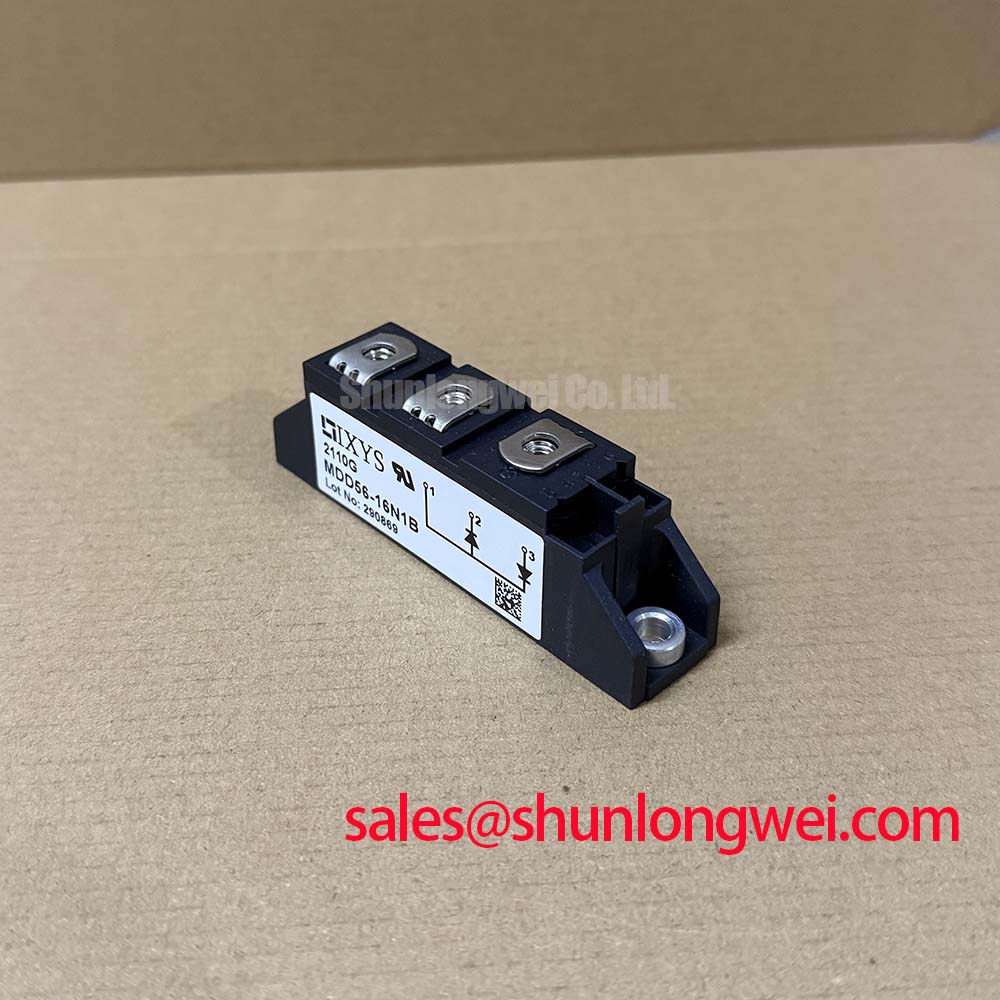
In a high voltage three phase motor solid state soft starter, technicians may encounter rectified auxiliary supplies, bypass control sections, or diode paths associated with power conversion assemblies. The 1600 V voltage rating and 56 A current rating of the MDD56-16N1B are Official Datasheet Specifications. They do not independently confirm suitability for a particular line voltage, overload profile, fuse arrangement, enclosure, or heatsink. Those conditions remain system determined.
Where phase controlled conversion is present, a change in firing angle changes the average transferred DC energy and the current waveform drawn from the AC source. At later firing angles, useful transferred power reduces while reactive demand and waveform distortion become more consequential. This is a Design Consideration rather than a specific characteristic claimed for this diode module. Engineers should capture line current and DC bus voltage during commissioning, then compare the observed waveform with the equipment’s documented operating state.
The module itself has no gate terminal and therefore has no gate trigger current or gate trigger voltage specification to tune. If the surrounding topology includes thyristors, their trigger pulse train, gate drive reference, and firing symmetry must be verified from the original controller documentation. Do not transfer thyristor gate parameters onto the MDD56-16N1B.
Fuse coordination also requires the actual protection documentation. The available official identification parameters establish voltage, current, and package type, but do not provide a fuse I²t coordination value. A semiconductor fuse must be selected and checked against the complete fault path, conductor capability, prospective short circuit current, and the protective limits documented for the host equipment. This is an Engineering Recommendation, not a factory fuse prescription for the module.
⚠️ Field Alert: Reconnect busbars only after confirming flat contact faces and tightening hardware to the equipment manufacturer’s specified torque, because uneven mechanical loading can compromise both electrical contact and thermal transfer.
When a repair bill of materials requires a separate comparison point, PD25016A can be reviewed as a distinct device record, but voltage class, current rating, circuit topology, terminal arrangement, thermal interface, and protection coordination must all be verified before any substitution is considered.
Benchtop Waveform Tuning: Mitigating Switching Stress in the MDD56-16N1B
Before changing snubbers or commutation components, inspect the waveform at the installed module terminals with measurement equipment appropriate for the circuit voltage and isolation requirements. Reverse recovery behavior can interact with commutation inductance, source impedance, switching device timing, and busbar layout. A sharp current transition, ringing voltage, or unexpected noise may indicate a system interaction that needs further measurement; it does not by itself establish a defect inside the diode module.
No official values for peak reverse recovery current, reverse recovery time, softness factor, or switching loss have been provided for the MDD56-16N1B. These figures must not be inferred from the 1600 V and 56 A ratings. The system integrator should obtain the applicable IXYS technical documentation or validate the installed assembly under controlled conditions before applying a recovery based switching calculation.
A practical bench sequence is to record the known good channel first, preserve probe position and ground arrangement, and then compare the suspected channel under the same load and firing conditions. Check commutation overlap, bus voltage excursion, and ringing frequency without moving directly to a single cause. Probe loop placement can create misleading high frequency detail, so the measurement setup should be reviewed before component changes are authorized.
Minimizing parasitic loop inductance is a Design Consideration when the objective is to suppress commutation overshoot and radiated switching noise. The required layout, damping, and permissible peak margins must be determined from switching tests against the actual DC link and protection architecture. For general reference on power semiconductor module roles and device families, see Shindengen Power Semiconductor Modules & Diodes.
In cabinets where a rectifier stage and an associated power conversion stage are serviced together, the circuit record for 6RI30G-160 can be consulted separately. It should not be treated as an automatic companion or replacement. Confirm its function, terminal map, ratings, and mechanical arrangement in the host assembly.
Benchtop Waveform Tuning: Mitigating Stress via Junction-to-Heatsink Heat Dissipation in the MDD56-16N1B
Remove power, allow the assembly to reach a safe handling condition, and examine the module mounting face and heatsink before blaming a thermal issue on the semiconductor. The MDD56-16N1B is specified as a module package, but no official junction to case thermal resistance, case to heatsink thermal resistance, baseplate planarity requirement, mounting torque, or permitted junction temperature value has been supplied here. Those values must not be invented during repair documentation.
A useful inspection starts with the old thermal interface pattern. Gaps, dry zones, embedded debris, or concentrated contact marks can point to an interface condition worth correcting. Clean both mating surfaces using methods approved for the equipment, apply the thermal interface material in accordance with the original assembly process, and tighten the mounting hardware using the module manufacturer’s applicable documentation. This is a Design Consideration for maintaining even contact pressure, not an official mounting specification for this model.
Thermal testing should compare temperatures and loading conditions that are genuinely comparable. A heatsink temperature reading alone cannot establish junction temperature, and a higher surface reading can arise from airflow changes, load changes, adjacent heat sources, or altered thermal contact. Where the system permits, observe phase current, ambient conditions, fan operation, and heatsink temperature trend together. The final thermal acceptability decision belongs to the system engineer responsible for the complete assembly.
Do not assume that a diode module supports double sided cooling, pressure disc hardware, or disc spring calibration. Those construction details are not established by the supplied MDD56-16N1B specifications. Use only the mounting method defined for the actual module housing and equipment chassis.
Transient Dynamics & Electrical Design: Saturable Reactor and Snubber Sizing for the MDD56-16N1B
When repetitive voltage peaks appear during commutation, trace the installed path first: diode terminals, busbars, fuse connections, capacitor connections, snubber components, and the adjacent switching device. Loose hardware, long conductor routes, degraded capacitors, or an altered layout can all affect observed transient behavior. The MDD56-16N1B rating of 1600 V remains an Official Datasheet Specification, while the acceptable transient profile must be verified within the complete system.
RC snubbers and series saturable reactors are system level elements, not intrinsic features confirmed for this module. Their selection is an Engineering Recommendation based on the measured commutation waveform, source inductance, capacitor behavior, switching sequence, thermal duty, and protection response. Designers should minimize unwanted loop inductance to reduce inductive overshoot, then verify peak voltage and current margins during switching tests. No resistor value, capacitance, or reactor characteristic should be copied into a repair simply because another cabinet uses a similar power rating.
Inspect creepage and clearance in the actual assembly whenever busbars, fuses, or snubbers are replaced. The required spacing depends on the installation standard, pollution environment, conductor geometry, insulation system, and equipment voltage category. The 1600 V rating of the module does not independently define the cabinet’s spacing compliance or insulation reliability.
For broader troubleshooting context involving industrial power conversion and semiconductor duty, consult Industrial Applications. Apply that material alongside the original soft starter drawings, approved protection scheme, and measured site waveforms when evaluating the MDD56-16N1B in service.