


Content last revised on September 22, 2026
FS150R12KT3 Operational Boundaries: Optimizing Heatsink Contact Pressure and Limits
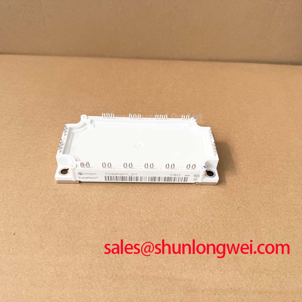
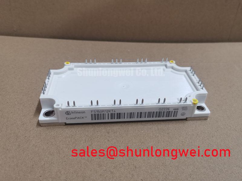
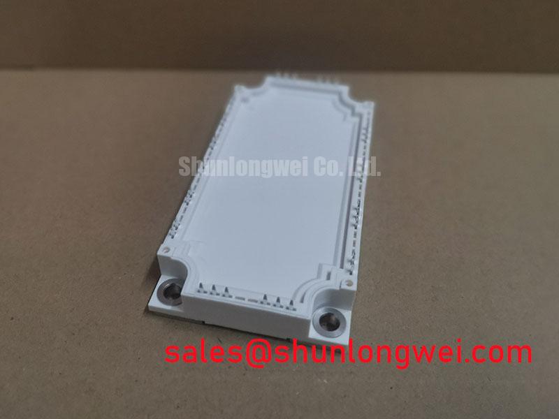
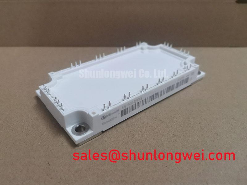
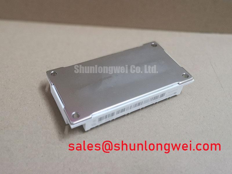
Begin the mechanical inspection with the heatsink surface, mounting points, insulating interface, and terminal hardware. Dust accumulation, uneven contact, aged thermal interface material, or a distorted baseplate interface can increase the thermal path even when the electrical connections appear correct. The module’s official electrical ratings are fixed specifications, while the usable current in an assembled inverter depends on switching frequency, conduction duty, ambient temperature, airflow, heatsink performance, and the complete thermal resistance path.
Design Consideration: Apply the thermal interface material as a continuous, controlled layer that fills surface irregularities without leaving visible voids or creating excessive squeeze-out during fastening. The exact interface thickness and fastener torque should come from the module mechanical drawing, the selected heatsink documentation, and the assembly standard used by the equipment manufacturer. If those documents are unavailable, the maintenance team should not treat a generic torque value as an official parameter for this module.
Use a sequential mounting process so that the baseplate seats progressively against the heatsink rather than being pulled down at one corner. Check the mating surfaces for burrs, contamination, and local high spots before applying the interface material. Clearance around power terminals should allow the busbar or cable lug to sit flat without applying mechanical force to the module body. A terminal that is forced into alignment can transfer stress to the internal connection structure and may also change the contact resistance during thermal cycling.
For field service, record the heatsink condition, fan or coolant status, terminal condition, and temperature rise under a repeatable operating point. A rising contact temperature should be investigated alongside airflow, load current, switching behavior, and interface condition rather than assigned to one cause without measurement. Infrared inspection can help locate abnormal thermal distribution, but emissivity, reflections, and exposed metal surfaces must be considered before interpreting the image.
The freewheel diode characteristics are also relevant to the switching loop. Reverse recovery softness, often represented by a device specific softness factor, can affect voltage overshoot and radiated noise. The value should be verified from the applicable Infineon documentation rather than inferred from the product family name. The Infineon IGBT Modules & Discretes Official Portfolio provides the manufacturer’s broader product context for engineers comparing module technologies.
⚠️ Maintenance Note: Check heatsink cleanliness, thermal contact condition, and terminal tightness during scheduled maintenance while monitoring contact temperature under a known operating load.
FS150R12KT3 Operational Boundaries: Evaluating Dynamic Power Loss and Thermal RC Limits
Dynamic loss evaluation should begin with measured switching waveforms and the actual operating profile rather than with the nominal 150.0 A rating alone. In a storage inverter, current may vary with battery state, grid support commands, reactive power, modulation index, and ambient conditions. The thermal model therefore needs to reflect conduction intervals, switching transitions, overload duration, and cooling response.
Engineering Recommendation: Use the manufacturer’s published conduction and switching data, where available, with the measured gate drive and commutation conditions of the host design. A multi RC thermal model can then estimate the transient case and junction response during pulsed operation. The resulting peak junction estimate must be checked against the applicable official limit and validated with case temperature measurements or an approved test method. A calculated result is an engineering calculation, not an additional FS150R12KT3 factory rating.
Phase angle control and line frequency ripple can produce a different thermal profile from steady sinusoidal current. When the converter processes uneven power, the heatsink may respond slowly while the semiconductor junction experiences shorter thermal excursions. The design team should evaluate the worst credible combination of current, switching state, DC link condition, ambient temperature, and cooling degradation. Thermal measurements should be synchronized with electrical waveforms so that a low average heatsink temperature is not mistaken for a safe junction condition.
RC snubbers, clamp networks, and gate resistance influence switching loss and voltage stress. Their values must be selected from the actual commutation loop, parasitic inductance, switching speed, and measured overshoot. A snubber that reduces a voltage spike may increase turn on or turn off loss, while excessive damping can alter control performance and thermal loading. Engineers should tune these networks on a controlled test bench and verify the result at the intended DC link voltage and load range.
For a replacement assessment, compare the original module’s gate drive behavior, freewheel path, busbar arrangement, and cooling interface with the replacement installation. The FS100R12N2T4 may appear in the same equipment evaluation because it is another module reference, but electrical compatibility, current capability, switching behavior, mechanical fit, and protection settings must be confirmed independently. A similar voltage class does not establish interchangeability.
Where the converter uses a separate input rectifier stage, the system integrator may also evaluate the FZ3600R12HP4 as a related rectifier stage reference. That relationship is a topology consideration only; it does not define a mandatory pairing or guarantee compatibility with the FS150R12KT3.
FS150R12KT3 Circuit Protection & Reliability: Planar Symmetrical Busbar Geometry
Inspect the commutation path from the DC link to the module terminals as a complete current loop. Wide, closely coupled forward and return conductors generally help reduce parasitic inductance, but the final geometry is determined by the converter’s voltage, current, switching speed, insulation system, creepage requirements, and mechanical construction. Keep the high di and dt loop compact without compromising required clearance or service access.
The familiar engineering relationship between peak voltage, DC link voltage, stray inductance, and current transition rate explains why a fast switching event can exceed the static voltage expectation. In practice, the team should measure the voltage directly at the module terminals with a suitable differential probe and compare it with the DC link waveform. Probe loop area, bandwidth, grounding method, and measurement position can otherwise create a false overshoot or hide a real one.
Planar busbars should be checked for symmetry, unwanted current crowding, sharp corners, loose laminations, and unintended coupling into signal wiring. The required creepage distance and electrical clearance are system insulation decisions governed by working voltage, pollution environment, altitude, material group, and applicable equipment standards. The module’s 1200.0 V rating does not by itself certify the assembled inverter insulation system.
MOVs, DC link capacitors, active clamps, and RC snubbers should be coordinated as one protection network. A MOV must be selected for the actual continuous operating voltage and transient energy environment; its clamping behavior, aging, and fault mode should be reviewed with the upstream fuse and enclosure design. A snubber capacitor is not sized from voltage rating alone because its pulse current, loss, layout inductance, and thermal behavior affect performance.
Long motor cables or remote load connections can create transmission line effects and reflected wave stress. When such cabling is present, verify the voltage at the inverter output terminals and at the motor or load end under the real cable length and termination condition. Output filtering may be appropriate, but the filter’s effect on control stability, common mode current, motor insulation, and semiconductor switching loss must be tested by the system designer.
Fast semiconductor fuses should be coordinated with the module’s short circuit withstand capability and the available fault energy. The fuse I squared t characteristic, clearing time, DC link capacitance, gate shutdown delay, and physical fault path all affect the result. Do not infer a safe dead short circuit duration from the 150.0 A continuous rating. Use the applicable manufacturer curves and validate the protection sequence with controlled testing.
Benchtop Waveform Tuning: Mitigating Stress from Atmospheric Neutron Radiation Effects on FS150R12KT3
Atmospheric neutron effects and single event burnout require a documented device qualification source and an application specific reliability assessment. They should not be converted into a specific FIT rate, altitude derating value, or guaranteed operating lifetime without authoritative data for the exact semiconductor technology, voltage condition, package, field environment, and mission profile. The official 1200.0 V rating is an electrical specification; it is not a published neutron immunity or SEB guarantee.
Design Consideration: If the equipment will operate at elevated altitude or in an environment where radiation reliability is a formal requirement, the system owner should request applicable manufacturer qualification information and perform a risk assessment against the real DC link voltage, transient margin, exposure profile, and protection response. Any proposed voltage headroom adjustment should be determined by the system reliability team and verified through documented analysis or testing.
Benchtop waveform tuning remains useful for ordinary electrical stress control. Capture turn off voltage, gate emitter behavior, diode recovery, common mode displacement, and DC link ripple using measurement equipment appropriate for the converter voltage. Compare the waveform at light load, rated load, regenerative operation, and the highest expected DC link condition. A clean waveform at one operating point does not establish safe behavior across the full modulation and temperature envelope.
During fault testing, confirm that the gate driver can command the required shutdown sequence and that the desaturation, overcurrent, fuse, and DC link discharge functions operate together. Keep the module isolated from uncontrolled energy during initial tests. After a suspected abnormal event, inspect the power terminals, gate circuit, snubber components, MOV condition, fuse response, and insulation path before applying another high energy pulse.
For structured troubleshooting and preventive inspection, engineers can consult the Field Engineer’s Handbook. It can support a measured workflow covering waveform capture, thermal checks, electrical isolation, and failure documentation without replacing the manufacturer’s official product data.
The Infineon IGBT Modules Overview is a suitable manufacturer reference when reviewing module families, application boundaries, and documentation requirements before integrating the FS150R12KT3 into a commercial string inverter or micro grid energy storage system.