
Content last revised on October 29, 2026
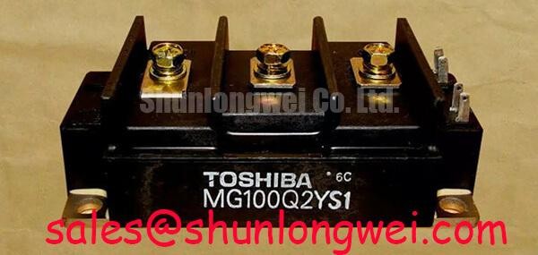
Toshiba MG100Q2YS1 Overview and Initial Inspection
With the DC link isolated and verified discharged, disconnect the gate connections before comparing collector-to-emitter and gate-to-emitter resistance readings on the removed MG100Q2YS1. Record the meter polarity and compare both switching positions; a resistance difference is a screening observation, not a complete failure diagnosis. Inspect the terminals, mounting surface, and original driver board before fitting another module.
The Toshiba MG100Q2YS1 is a 2-pack half-bridge IGBT module with a collector-emitter voltage rating of 1200 V and collector current rating of 100 A at a case temperature of 25°C (Official Specification). Its specified typical collector-emitter saturation voltage is 2.7 V; this is a characteristic under datasheet test conditions, not a constant operating voltage. The specified isolation withstand is 2500 V AC for one minute, a test rating rather than permission to omit system insulation checks.
MG100Q2YS1 Operational Boundaries: Evaluating High-Speed Fault Management: V_CE Desaturation Limits
Trace the desaturation sensing path from each collector connection to the driver protection input before attempting powered operation. As a Design Consideration, contamination, damaged sensing components, or an interrupted return connection can affect the apparent collector-emitter voltage seen by the protection circuit. Compare the sensing network with the equipment schematic and inspect its separation from high-current switching conductors.
Separate fault-on-turn-on events from faults developing after the IGBT is already conducting. These conditions place different demands on blanking, detection, and shutdown behavior. The protection timing must coordinate sensing delay, driver propagation, and gate discharge with the applicable short-circuit safe operating area. A generic microsecond target does not establish the MG100Q2YS1 short-circuit withstand capability; use the device’s documented conditions when assessing the original driver.
For a driver incorporating two-stage soft turn-off, inspect the intermediate discharge path and final gate pull-down independently. As a Design Consideration, slowing fault-current interruption can reduce inductive overshoot, but excessive delay prolongs semiconductor stress. Capture collector-emitter voltage, gate-emitter voltage, and the protection signal with appropriately rated differential measurement equipment during controlled commissioning. The relevant result is coordinated shutdown without exceeding the device’s electrical boundaries, not simply a clean-looking gate trace.
Check whether an apparent desaturation trip coincides with complementary-device switching. Miller coupling through collector-gate capacitance can disturb the off-state gate, while common wiring impedance can distort the measured gate voltage. Reverse-transfer capacitance and Miller plateau charge are related switching characteristics, but they are not interchangeable quantities. The article Evolution of Negative Off-Bias Gate Drive Circuits provides background for evaluating the existing off-state drive arrangement without prescribing a different bias voltage.
Dead time, active Miller clamping, and any collector-voltage active clamp should be assessed as separate functions. Excessive overlap can produce cross-conduction; excessive dead time can extend diode conduction and change commutation behavior. Diode reverse-recovery softness also influences ringing, but a softness factor cannot be assigned to this module without supporting characteristics. Keep gate and sensing loops away from power-loop coupling, with final separation and timing determined by the equipment’s insulation requirements and measured switching behavior.
Benchtop Waveform Tuning: Mitigating Stress via Baseplate Convexity Inspection on MG100Q2YS1
Check the module mounting surface and heatsink contact face for contamination, raised edges, and damage before interpreting temperature-dependent waveform changes. As a Design Consideration, surface curvature should be evaluated against the applicable mechanical drawing rather than treated automatically as a defect. Do not flatten, grind, or force the module against a heatsink to correct an assumed dimensional problem.
Use the specified mounting sequence and calibrated tooling to develop even contact pressure. Where a diagonal tightening sequence is prescribed, increase clamping progressively rather than fully tightening one corner first. Select the thermal interface material and application method from the approved assembly instructions; an arbitrary thickness does not establish satisfactory contact. Field Alert: Do not use mounting screws to pull an uneven module base onto the heatsink; resolve the contact problem before tightening.
After mounting, correlate case-temperature behavior with load and cooling conditions rather than judging the interface from expelled compound alone. Heatsink conduction and airflow remain central to this check. The Stefan–Boltzmann law for radiative heat exchange describes an additional enclosure heat-transfer mechanism, but it does not determine the module-to-heatsink thermal resistance or replace contact inspection.
For an existing bootstrap-powered high-side driver, examine supply droop throughout the longest commanded on-state. As an Engineering Recommendation, capacitor sizing should account for gate charge, driver quiescent consumption, leakage, permissible supply variation, and recharge opportunities. Also inspect the charging path and driver undervoltage response. A supply disturbance can change switching behavior even when the control command remains correct.
When evaluating this module for a heavy-duty variable-frequency AC motor drive, compare the mechanical drawing, terminal arrangement, gate-drive requirements, diode characteristics, and thermal limits against the original assembly. The BSM100GB120DLC can be included in a documented cross-model assessment, but matching headline voltage and current does not establish interchangeability. Preserve the distinction between an electrical candidate and a mechanically and dynamically verified replacement.
MG100Q2YS1 Operational Boundaries: Evaluating Dynamic Braking Chopper Operation Limits
Locate the actual braking switch and resistor connections on the equipment schematic before attributing a deceleration overvoltage trip to the MG100Q2YS1. Its half-bridge configuration does not establish an integrated braking function. During regeneration, energy enters the DC link; a braking chopper controls current into a resistor, where that energy is dissipated as heat.
As a Design Consideration, brake-switch evaluation should include repetitive current, switching stress, thermal loading, and the available operating-area information. Resistor assessment should cover resistance tolerance, pulse-energy capability, repetition rate, cooling, and thermal protection. Mechanical load inertia and the commanded deceleration profile determine the energy demand, so resistor selection cannot be derived from the module’s current rating alone.
During troubleshooting, compare the DC-link waveform with the braking command and resistor-current response. Inspect disconnected resistors, degraded connections, inhibited drive signals, and thermal interlocks as separate possibilities. Keep the chopper current loop compact to limit switching overshoot, while maintaining the equipment’s required electrical clearances. Any MOV or snubber network should be assessed for its documented transient role; it is not a substitute for a braking resistor capable of absorbing the required energy.
Map adjacent conversion stages without assuming their functions from part numbers. The MG300Q1US41 is a separate module to assess against its own circuit position and specifications, not an automatically compatible rectifier or braking companion. Likewise, an interleaved boost converter can reduce input-current ripple through phase interleaving, but that topology alone does not establish a regenerative energy-return path. Resolve the deceleration fault by verifying the installed energy-disposal path and its thermal protection under the equipment’s approved test procedure.