

Content last revised on October 31, 2026
Transient Dynamics & Electrical Design: Auxiliary Emitter Pinout Cold-Check on MG75J1BS11
With the DC link isolated and verified discharged, trace the MG75J1BS11 gate return against the equipment schematic before connecting a replacement module or attaching an oscilloscope probe. A continuity reading between emitter connections cannot establish which connection belongs in the driver return path; terminal identification and the physical current route must agree with the module connection drawing.
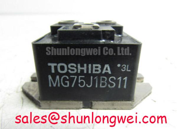
The Toshiba MG75J1BS11 IGBT module has an Official Specification of 600 V collector-emitter voltage and 75 A continuous collector current at a case temperature of 25°C. Its specified typical collector-emitter saturation voltage is 2.1 V, maximum power dissipation is 400 W per element, and junction temperature range is −40 to +150°C. The saturation voltage is a typical characteristic, not a guaranteed worst-case loss value; the dissipation rating is not a continuous operating target independent of cooling conditions.
Identify the main emitter connection from the terminal drawing, then establish whether the actual module connection arrangement provides a separate auxiliary emitter return. A dedicated Kelvin emitter must not be inferred from the model name or from multiple terminals showing continuity. Where a separate driver return is documented, trace it directly to the gate-driver reference rather than routing it through the load-current conductor.
Design Consideration: Shared emitter inductance develops a voltage during changes in load current, altering the gate-emitter voltage experienced by the device. A driver referenced to the wrong physical point can therefore show an apparently acceptable output waveform while the voltage at the module differs. Inspect conductor routing, connector assignments, solder joints, and return-path continuity with the driver disconnected as appropriate to the equipment service procedure. Compare suspicious readings with the schematic rather than assigning a universal resistance threshold.
Keep gate and return conductors close together to limit the enclosed loop area, while maintaining the equipment’s required electrical clearances from power conductors and exposed metalwork. Route the pair away from switching nodes wherever the assembly permits. Short wiring alone is not sufficient if the return shares a segment carrying commutating current. During waveform checks, place the differential measurement across the relevant gate and emitter connections; a remote control-board ground can conceal or exaggerate local disturbance.
The 600 V collector-emitter rating defines a device boundary, not a prescribed DC-link operating voltage. Assess bus voltage together with switching overshoot and the intended operating envelope. The IGBT Design & Integration reference provides supporting context for relating gate-drive layout, commutation paths, and thermal constraints during that assessment.
Pro Tip: Keep outgoing and return commutation paths closely coupled and geometrically balanced where practical, then verify turn-off voltage margin with a controlled double-pulse test representative of the intended operating conditions.
Preventing Spurious Faults: Thermal Interface Material Thickness Uniformity Guidelines for MG75J1BS11
Inspect heatsink flatness, interface cleanliness, and the previous mounting contact pattern before applying fresh thermal interface material. Uneven contact can create a localized temperature rise even when the accessible heatsink surface appears satisfactory. Remove residue without damaging the mating surfaces, inspect for burrs, and investigate visible rocking or distortion rather than attempting to compensate with extra tightening force.
Design Consideration: Select the interface material and compressed bond-line thickness for the actual surface condition and mounting arrangement. A thin, continuous interface should fill surface irregularities without becoming an unnecessarily resistive thermal layer. The required thickness depends on material behavior, surface flatness, and assembly pressure; it is not established by the module’s electrical ratings. Use the material supplier’s application method and inspect coverage for voids or displaced regions.
Bring the mounting fasteners into contact progressively, following the approved assembly sequence and specified torque for the actual hardware. Uneven tightening can tilt the mounting surface and redistribute interface material. Baseplate curvature should be assessed against the mechanical requirements rather than forcibly flattened. Press-pack clamping, disc-spring calibration, and double-sided cooling procedures should not be transferred to this module without an explicitly documented mechanical arrangement.
The 400 W per-element dissipation specification does not establish an allowable heatsink temperature by itself. Thermal assessment must account for conduction loss, switching loss, interface resistance, and the cooling system’s operating conditions. Likewise, the 2.1 V typical VCE(sat) value cannot represent loss across every current and junction temperature. When investigating intermittent thermal trips, compare temperature trends with load and switching activity before attributing the event to the interface.
During replacement assessment, compare electrical and mechanical compatibility together. The CM75E3Y-12E can be included in a cross-model review, but its inclusion does not establish interchangeability with MG75J1BS11. The following comparison separates the specified MG75J1BS11 ratings from characteristics requiring a datasheet-to-datasheet check.
| Selection criterion | Toshiba MG75J1BS11 | CM75E3Y-12E comparison requirement |
|---|---|---|
| Collector-emitter voltage | 600 V — Official Specification | Consult datasheet for rating and test conditions |
| Continuous collector current | 75 A at Tc = 25°C — Official Specification | Compare current rating at equivalent case temperature |
| Collector-emitter saturation voltage | 2.1 V typical — Official Specification | Compare at matching current, gate voltage, and temperature |
| Maximum power dissipation | 400 W per element — Official Specification | Compare thermal limits and stated boundary conditions |
| Junction temperature range | −40 to +150°C — Official Specification | Compare operating limits |
| Integration compatibility | Check terminal drawing and mounting outline | Match topology, connections, footprint, and driver requirements |
For a commercial string inverter or micro-grid energy-storage converter, compatibility evaluation should also address the existing modulation strategy and current ripple. Line-frequency ripple changes the instantaneous loading that contributes to heating; phase-angle conduction control should be considered only where it actually belongs to the host circuit. An RC snubber is a system-level transient-control element whose placement, dissipation, and interaction with switching must be evaluated separately, not a remedy for poor thermal contact.
Field Diagnostics & Commissioning: High dv/dt Cross-Conduction Shoot-Through in MG75J1BS11 Topologies
Capture the nominally off device’s gate-emitter voltage while the opposing switch commutates, and correlate any disturbance with collector-emitter voltage and current. A gate excursion alone does not prove shoot-through: probe coupling, emitter-reference movement, diode recovery, and actual unintended channel conduction can produce overlapping symptoms. Use appropriately rated differential instrumentation and compare timing across the relevant signals.
Design Consideration: Miller capacitance couples collector voltage transitions into the gate circuit. A low-impedance turn-off path can help remove that coupled charge, while a suitably implemented active Miller clamp can constrain gate movement near the off state. Evaluate clamp placement and its return path at the device terminals. Negative gate bias is another system-dependent option, but its magnitude must remain compatible with the device’s gate limits and driver behavior, including startup and loss-of-supply conditions.
Check commanded dead time against actual switching behavior across load and temperature. Driver propagation differences and turn-off tails can reduce the effective non-overlap interval, whereas excessive dead time can increase diode conduction and associated loss. The system designer should establish timing from measured behavior, not assign a universal interval from the module’s current rating. Repeat observations after changes to gate resistance, driver hardware, or commutation components.
Review desaturation protection as a coordinated sensing and shutdown function. The specified 2.1 V typical saturation voltage is not itself a desaturation trip threshold. Blanking must reject normal switching transitions without concealing a developing fault, and soft shutdown must balance fault-current interruption against collector overvoltage. Short-circuit safe operating area and permitted fault duration require their own device-specific basis; ordinary voltage and current ratings do not establish either.
Where the surrounding converter uses separate freewheeling diodes, their commutation behavior also belongs in the investigation. Wolfspeed Silicon Carbide Schottky Diodes provides authoritative background on that separate diode technology; it does not establish the internal diode construction or recovery characteristics of MG75J1BS11. Assess the installed power path as a whole, then confirm that the corrected gate waveform, protection response, and collector-voltage peak remain acceptable throughout the intended commissioning envelope.

