
Content last revised on September 10, 2026
MG150Q2YS11 Replacement Checks and Key Ratings
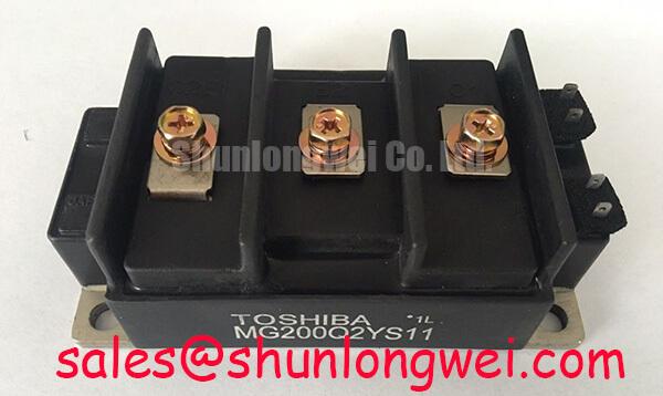
Before energizing a replacement, isolate the assembly, inspect the package and terminals, then verify the nameplate limits against the original inverter design. The Toshiba MG150Q2YS11 is a high-power IGBT module specified for a 1200 V collector-emitter voltage rating and a 150 A DC collector-current rating. It should be evaluated against the switching waveform, cooling path, gate-drive arrangement, and mechanical interface of the equipment being repaired rather than treated as a drop-in match by current rating alone.
The published electrical data identifies a collector-emitter saturation voltage of 4.0 V at IC = 150 A and VGE = 15 V, a diode forward voltage of 3.5 V at IF = 150 A and VGE = 0 V, and a typical turn-off time of 0.6 µs. These values are Official Specification data. Actual operating loss depends on switching frequency, current waveform, junction temperature, gate resistance, commutation behavior, and the parasitic inductance of the complete power stage.
| Parameter | Symbol | Value | Status |
|---|---|---|---|
| Collector-emitter voltage | VCES | 1200 V | Official Specification |
| Gate-emitter voltage | VGES | ±20 V | Official Specification |
| DC collector current rating | IC | 150 A | Official Specification |
| Collector power dissipation per transistor | PC | 1250 W | Official Specification |
| Collector-emitter saturation voltage | VCE(sat) | 4.0 V at IC = 150 A, VGE = 15 V | Official Specification |
| Diode forward voltage | VF | 3.5 V at IF = 150 A, VGE = 0 V | Official Specification |
| IGBT junction-to-case thermal resistance | Rth(j-c) | 0.1 °C/W | Official Specification |
| Diode junction-to-case thermal resistance | Rth(j-c) | 0.32 °C/W | Official Specification |
| Typical turn-off time | toff | 0.6 µs | Official Specification |
MG150Q2YS11 Thermal-Electrical Optimization: Transient Thermal Impedance and Practical Tuning
Thermal verification should begin at the case, not at the heatsink label. Measure or estimate case temperature near the module mounting area, then calculate conduction and switching losses using the actual current and duty waveform. The stated Rth(j-c) of 0.1 °C/W for the IGBT and 0.32 °C/W for the diode are steady-state junction-to-case specifications; they do not by themselves define the junction temperature during a short overload or repetitive energy-storage pulse.
For pulsed operation, designers should use the manufacturer’s available transient thermal data or an appropriate multi-RC thermal model when calculating peak junction temperature. The model should reflect pulse duration, repetition interval, case temperature, and the separate heat contribution from the freewheel diode. A commercial string inverter or micro-grid energy-storage converter may impose highly different thermal stress during DC-link charging, power transfer, regeneration, and fault recovery, so a single average-current calculation can conceal short thermal excursions.
During commissioning, compare calculated temperature with thermocouple or infrared measurements taken under a controlled load. Check the interface flatness, contact pattern, clamping uniformity, and heatsink airflow before changing gate-drive settings. The system engineer should also verify switching overshoot with a properly referenced differential probe, because excessive voltage stress can appear as a thermal problem after repeated switching events.
For related maintenance planning, the Field Engineer’s Handbook provides a broader reference for test planning and failure analysis. It should supplement, not replace, the Toshiba documentation for this device.
Preventing Spurious Faults: Galvanic Gate Drive Isolation and Reinforced Guidelines
The MG150Q2YS11 gate has a maximum gate-emitter voltage rating of VGES = ±20 V, making gate-voltage measurement and isolation verification essential during replacement work. The module rating does not certify the isolation barrier of a particular driver board. Designers should verify the gate driver’s reinforced insulation, creepage and clearance, common-mode transient immunity, and power-supply sequencing against the converter’s measured switching environment.
Gate-loop parasitic inductance can convert rapid collector-voltage transitions into unwanted gate-emitter excursions. Keep the driver return path compact, route the gate and emitter return as a controlled loop, and separate high-current commutation paths from sensitive control references. The correct gate resistance is system-dependent: it must be selected while observing turn-on loss, turn-off overshoot, gate ringing, diode recovery, and the driver’s source and sink capability.
Bootstrap gate supplies require similar verification. The capacitor must maintain adequate voltage during the complete high-side conduction interval, while the charging path and diode must tolerate the switching frequency, recharge current, and recovery behavior of the actual circuit. The system integrator should confirm the driver supply voltage from the original schematic and validate undervoltage-lockout timing before applying a high-voltage bus.
Thermal interface material should be applied consistently across the intended contact area, with thickness and compression governed by the module and heatsink assembly instructions. Use a controlled, cross-pattern fastening sequence where the mechanical design calls for it, then recheck mounting flatness and terminal stress. 💡 Pro Tip: Disconnect the DC link and gate-drive supply before inserting or removing any control connector.
Assembly Integrity and Layout Architecture: Active Miller Clamp Implementation
An active Miller clamp can reduce the risk of an unintended turn-on when the opposing switch experiences a fast collector-voltage transition. This is a Design Consideration for the gate-drive system, not an internal feature that can be assumed from the MG150Q2YS11 part number. The driver architecture, gate-emitter reference, clamp timing, and protection thresholds must be confirmed against the selected circuit.
Do not select a negative gate bias as a fixed prescription without testing the module, driver, isolation supply, and parasitic network together. A negative bias may improve noise immunity in some bridge layouts, but it also changes gate-emitter stress, driver power demand, and fault behavior. The maximum positive and negative gate-emitter limits remain ±20 V; switching measurements should confirm that ringing stays within those official boundaries under the worst credible operating condition.
During troubleshooting, observe both gate-emitter voltage and collector-emitter voltage with isolated, bandwidth-appropriate probes. A repeated fault may involve driver timing, isolation displacement current, diode recovery, common-emitter inductance, or a control interlock issue. Avoid assigning a single cause from a gate waveform viewed without the power waveform. Double-pulse testing or an equivalent controlled switching test can help the design team assess peak voltage and current margins against the DC-link condition.
For background comparison across power semiconductor technologies, engineers can consult the STMicroelectronics STPOWER IGBTs and Power Transistors resource and the Vishay Siliconix Industrial Power MOSFETs resource. These are industry references, not specifications for the Toshiba module.
Preventing Spurious Faults: Kelvin Emitter Connection Guidelines
Emitter-current sharing becomes difficult when the gate-drive return and the main power return use a common impedance. The MG150Q2YS11 installation should follow the original terminal assignment and mechanical drawing, with the driver reference connected according to the module topology. If the assembly provides a separate auxiliary emitter or Kelvin connection, keep that return dedicated to the driver loop and prevent high-current commutation current from passing through it.
Minimize the area of the gate-emitter loop and maintain physical separation between control wiring and the collector switching path. A symmetrical busbar arrangement can reduce unequal stray inductance in bridge legs, but the final layout must be validated by oscilloscope measurements at the module terminals. Look for gate ringing that changes with load current, unequal switch timing, or an emitter reference that moves during commutation; these observations may indicate mutual coupling or an unsuitable probing reference.
When a failed unit is being replaced in a field inverter, compare terminal identification, mounting footprint, gate-driver polarity, diode path, and protection logic before installation. The electrically related MG150Q1JS40 may be reviewed as a separate maintenance option, but compatibility must be established from its own datasheet and the equipment schematic. In the upstream rectifier or complementary power stage, engineers may also examine MG100Q1ZS40 as a related device without assuming pin, voltage, current, or switching equivalence.
After assembly, perform a low-energy gate-drive check, confirm the correct quiescent state, and inspect the switching waveform before applying the full DC link. The final acceptance test should cover insulation, gate-emitter limits, collector-emitter overshoot, thermal response, protection timing, and load transients under conditions representative of the commercial string inverter or micro-grid energy-storage system.