
Content last revised on October 30, 2026
Assembly Integrity & Layout Architecture: Implementing DC-Link Capacitance Bank Layout and Low-Inductance Connections for MG150Q2YS9
With the DC link discharged and isolation verified, inspect the module terminals, mounting interface, and local capacitor connections before investigating a power-stage trip. For the MG150Q2YS9, terminal damage, loose busbar joints, and a disturbed thermal interface deserve attention alongside semiconductor measurements; replacing the module alone does not establish that the surrounding circuit is ready to operate.
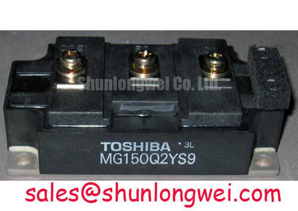
The Toshiba MG150Q2YS9 IGBT module has official specifications of 1200 V collector-emitter voltage and 150 A DC collector current. Its other official ratings include ±20 V gate-emitter voltage, a −40 to +150°C junction temperature range, and 2500 V AC isolation voltage for one minute. These limits address different electrical and thermal stresses; none should be treated as a normal operating target.
Official collector-emitter saturation voltage is 2.4 V typical and 3.0 V maximum, while collector power dissipation is 1100 W at a case temperature of 25°C. Consult the Toshiba datasheet for the saturation-voltage test conditions, terminal drawing, switching characteristics, safe operating areas, and mechanical installation requirements. Those details are especially important when assessing an existing assembly rather than reproducing its original configuration.
Trace the local commutation path from the DC-link capacitor bank through the switching module and back to the capacitors. Design Consideration: the relevant path is the fast switching loop, not simply the shortest visible cable. Closely coupled outgoing and return conductors can reduce loop inductance, whereas a compact capacitor bank connected through long, separated conductors can still leave substantial transient voltage at the module terminals.
Engineering Calculation: the first-order relationship Vpeak ≈ VDC + Lσ × |di/dt| explains why turn-off overshoot increases with commutation-loop inductance and current slew rate. This approximation identifies the layout variables worth investigating; it does not include every contribution from ringing, diode recovery, or clamping behavior. Compare the measured collector-emitter peak with the 1200 V rating under the actual DC-link and switching conditions, leaving the operating margin to the system qualification process.
Design Consideration: evaluate capacitor placement, connection inductance, ripple-current capability, and temperature together. A snubber capacitor should be selected from measured transient energy, repetitive dissipation, and the behavior of its complete connection path. Adding capacitance without examining damping can change ringing frequency without adequately controlling the peak. Position voltage probes so that the measurement loop does not become an additional source of apparent overshoot.
Planar busbar symmetry is useful when it produces comparable electrical paths, not merely matching outlines. Engineering Recommendation: inspect overlapping conductor regions, terminal transitions, and capacitor-bank connections for unnecessary loop area. Maintain creepage and clearance according to the equipment’s working voltage, insulation system, pollution conditions, and applicable product standard. The module’s 2500 V AC, one-minute isolation specification is not a substitute for assessing external terminal spacing or the complete assembly’s insulation coordination.
Practical tip: Keep the outgoing and return commutation paths closely coupled, then verify turn-off voltage margin with a controlled double-pulse test using the intended busbar and capacitor assembly.
When comparing related procurement options, MG300Q2YS50 can serve as a separate Toshiba reference in a compatibility worksheet, not as an assumed interchangeable replacement. Compare its voltage class, terminal arrangement, mounting geometry, gate-drive requirements, losses, and operating-area data independently. A related model designation does not establish electrical or mechanical equivalence.
MG150Q2YS9 Thermal-Electrical Optimization: Symmetrical Busbar Geometry for High-Current Practical Tuning
Compare branch currents and case temperatures under the same load before attributing unequal heating to device variation. Design Consideration: if an equipment design uses parallel modules, unequal busbar resistance, terminal contact resistance, cooling conditions, or driver timing can produce different current distributions. Symmetry should therefore cover both power connections and the paths that command switching.
A positive temperature coefficient of collector-emitter saturation voltage can support static sharing only within the operating region where that behavior is established. The MG150Q2YS9 saturation-voltage figures alone do not establish its temperature coefficient across load. Engineering Recommendation: examine temperature-dependent output curves before relying on thermal feedback for sharing, and distinguish steady-state conduction balance from switching-current balance. Equal average currents can conceal unequal transient stress.
Dynamic sharing depends on gate-loop impedance, propagation timing, device characteristics, and the power-loop geometry. Design Consideration: compare gate-emitter and collector-emitter waveforms between branches using consistent probe locations and loading conditions. Investigate a repeatable timing difference before changing individual gate components. Adjustments intended to correct one branch can alter switching loss or transient voltage elsewhere in the assembly.
The official 1100 W dissipation rating at a 25°C case temperature should be read as a specified thermal boundary condition, not as the heat that an installed heatsink can necessarily remove. Engineering Recommendation: estimate conduction and switching losses at the intended operating point, then assess junction temperature using the appropriate thermal impedance information. Check the hottest operating condition rather than relying on cabinet air temperature or an unloaded case measurement.
For broader thermal-interface concepts, The Advanced Thermal Management Revolution provides background on heat-flow paths and cooling approaches. That discussion should not be read as evidence that MG150Q2YS9 uses a particular substrate or cooling architecture. The practical task remains to characterize the installed module-to-heatsink path and its temperature rise.
Protection coordination also needs separate treatment. Design Consideration: compare a semiconductor fuse’s clearing characteristics and let-through energy with documented device and circuit withstand limits; the 150 A DC rating is not a surge-current or short-circuit withstand specification. Fuse operation can limit fault energy in the power path, while driver protection addresses the switching event on a different timescale. Desaturation detection, blanking, fault propagation, and controlled turn-off should be evaluated together so that detection rejects normal switching transients without allowing excessive fault stress.
Preventing Spurious Faults: Auxiliary Emitter Return Trace Separation Guidelines for MG150Q2YS9
Follow the gate-driver return connection to the emitter reference shown in the terminal drawing before modifying the wiring. Design Consideration: shared impedance between load current and the driver return can shift the effective gate-emitter voltage during switching. Where an assembly provides a separate signal-return route, keep it distinct from the high-current conductor; do not assume that MG150Q2YS9 contains a dedicated internal Kelvin-emitter connection.
Keep the gate command and its return closely associated along their external route. Engineering Recommendation: assess connector transitions, driver-board placement, and proximity to switching nodes as one circuit. A short gate lead with a distant return can still have an unfavorable loop. Creepage and clearance around this wiring must satisfy the equipment’s insulation requirements rather than an arbitrary spacing rule.
Miller coupling provides another route for unintended gate movement. Design Consideration: collector-voltage transitions drive displacement current through the gate-collector capacitance, and the resulting gate excursion depends on the driver’s sink behavior and return impedance. Review the gate waveform at the module connection during complementary switching. The official ±20 V gate-emitter limit defines a boundary; it does not prescribe the driver’s operating voltages.
Active Miller clamping and collector-voltage clamping address different stresses. Engineering Recommendation: evaluate any Miller clamp against the actual gate excursion and driver return path, while evaluating collector clamping against turn-off energy and voltage overshoot. Neither should be treated as a substitute for correcting a poorly controlled commutation loop. If desaturation protection operates intermittently, examine the sensing path and switching waveforms before changing its threshold or blanking behavior.
For semiconductor background, the discussion of trench-gate and field-stop IGBT technology explains general architectural developments; it does not establish the internal architecture of MG150Q2YS9. Likewise, background on fluxgate sensing principles can help explain a measurement method, but a particular current transducer still requires its own bandwidth, offset, and calibration assessment.
Design Consideration: where a commutation diode participates in the power stage, reverse-recovery current can affect collector overshoot and measured gate disturbance. Compare current and voltage transitions together rather than diagnosing the disturbance from a gate trace alone. Do not assign a reverse-recovery softness factor or switching-loss value without component-specific data, and do not infer equipment-level EMC compliance from an apparently clean local waveform.
Transient Dynamics & Electrical Design: Heatsink Surface Flatness and Thermal Grease on MG150Q2YS9
Inspect the heatsink contact surface for burrs, embedded particles, damaged threads, and residual interface material before placing the module. Engineering Recommendation: evaluate flatness and the module’s mating surface against the installation drawing rather than attempting to straighten the package by tightening its fasteners. Local contact defects can produce uneven pressure and a thermal bottleneck even when the assembly appears secure.
Apply the thermal interface material using the material supplier’s process and the module’s mounting requirements. Design Consideration: the objective is consistent contact with limited voiding, not a universally prescribed grease thickness. Account for surface finish, interface-material behavior, and application repeatability. Avoid assigning a fixed coating thickness to MG150Q2YS9 without a supported assembly specification.
Use a calibrated fastening tool and the documented torque, fastener, and tightening sequence. Engineering Recommendation: where the approved procedure calls for progressive diagonal tightening, increase clamping pressure evenly rather than fully loading one corner first. Mounting screws and electrical-terminal fasteners perform different functions and should not inherit the same torque by assumption. Record the assembly procedure so that later temperature comparisons have a meaningful mechanical baseline.
After installation, assess temperature rise at repeatable load and cooling conditions, checking that sensor attachment and measurement location remain consistent. Design Consideration: a rising case temperature can reflect interface resistance, airflow restriction, coolant conditions, or increased semiconductor losses; distinguish these possibilities through correlated electrical and thermal measurements. The 150°C maximum junction temperature is not directly demonstrated by a heatsink reading.
For compatibility assessment in industrial inverter welders or medium-frequency induction-heating power supplies, engineers should compare the actual switching frequency, resonant or hard-switching behavior, cooling arrangement, and protection response with the module’s operating limits. Engineering Recommendation: after thermal stabilization, repeat the relevant switching measurements and inspect the interface if temperature distribution remains uneven. This checks whether the repaired assembly maintains both electrical margin and a reproducible heat-transfer path.