
Content last revised on September 10, 2026
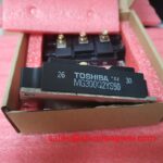
Benchtop Waveform Tuning: Mitigating Stress via Dynamic Gate Impedance Control for Robust Operation on MG300Q2YS50
Before applying full DC-link power, check the gate-drive output with the module disconnected where the equipment design permits. Confirm that the driver transitions cleanly, that its return reference is intact, and that no unexpected control pulse appears during controller startup, shutdown, fault reset, or auxiliary-supply sequencing. In a damaged commercial string inverter or micro-grid energy storage converter, a gate signal that appears acceptable at low voltage may still become unstable after the power stage is connected because fast switching current can disturb the local emitter reference.
Design Consideration: rapid collector-voltage movement can couple through the device’s internal gate-related capacitances and raise the effective gate voltage of the opposing switch. If that voltage reaches the driver’s turn-on region while the other position is conducting, cross-conduction can occur. An active Miller clamp is often evaluated as a low-impedance path holding the inactive gate close to its local emitter reference after turn-off. Negative gate bias is also a common gate-drive technique, but its exact voltage range must be selected from the applicable device documentation, driver limits, isolation rating, and measured switching behavior. It must not be copied from an unrelated IGBT module design.
At the bench, use differential voltage probing and correctly referenced current measurement to observe turn-on and turn-off at progressively controlled operating conditions. Look for gate ringing, delayed turn-off, an inactive gate rising during the companion device transition, or collector-voltage overshoot that changes materially with cable position. Any of these observations may indicate a return-path problem, insufficient gate damping, excessive shared inductance, or a driver fault. They do not establish a single cause without waveform comparison against a known-good channel or a validated design target.
Where the original inverter documentation identifies a separate auxiliary emitter or driver return terminal, preserve that routing during repair. Do not join that return into a convenient high-current copper path merely because continuity testing shows both nodes connected at DC. Their behavior during switching can be very different. For current-class comparison during evaluation, the MG100Q1ZS40 should be treated as a separately documented module, not as an automatic substitute for MG300Q2YS50.
⚠️ Field Alert: Disconnect control power and verify that stored energy is discharged before reconnecting any gate-drive or power-terminal cable.
Transient Dynamics & Electrical Design: Thermal Stress Alleviation in Bidirectional Operation on MG300Q2YS50
In commercial string inverter and micro-grid energy-storage equipment, a bidirectional conversion stage can transfer energy between battery racks and an inverter DC link. During charge, discharge, peak shaving, and grid-support transitions, the direction of power flow and the thermal distribution within the bridge can change. The official 1200 V and 300 A ratings of MG300Q2YS50 are essential boundaries for equipment identification, while actual operating stress depends on the DC-link voltage, current waveform, switching conditions, cooling path, control strategy, and fault response implemented by the host system.
When investigating repeated trips after a battery charge or discharge event, inspect whether both parallel paths share current in a comparable manner. Design Consideration: IGBT conduction characteristics can exhibit a positive temperature coefficient over relevant operating regions, which can support static current sharing when matched modules, equal thermal conditions, and symmetrical interconnects are used. It does not remove the need to inspect busbar symmetry, driver timing, current-sensor placement, and cooling contact. A hotter device can be the result of unequal switching loss, a poor heatsink interface, airflow variation, or a control imbalance rather than a direct indication of module failure.
Use recorded controller alarms, thermal sensor trends, and phase-current captures to identify whether the event follows a specific power-flow direction or a particular bridge position. If the host equipment includes a temperature-sensing network, verify the sensor path and controller interpretation against the equipment documentation. A thermistor is a temperature-sensitive resistor; its general operating principle is described in this technical reference on thermistors. That reference does not confirm that MG300Q2YS50 contains a particular sensor or temperature-monitoring structure.
Thermal cycling should be addressed through measured case temperature, cooling-system condition, controlled load testing, and examination of mounting contact. Avoid estimating service life from a single overload event or from elapsed operating hours. No field-life figure can be assigned to this module without an applicable test method, system mission profile, and sourced reliability evidence. For maintenance teams handling intermittent inverter faults, the Field Engineer’s Handbook provides a useful structured path for electrical isolation checks, waveform capture, and evidence-based failure analysis.
In converter systems where a separate power stage is being assessed as part of the same cabinet-level architecture, the MG150Q1JS40 can be reviewed as another documented module reference. Its presence in a related topology does not establish electrical interchangeability, equal current capability, or equivalent gate-drive behavior.
Assembly Integrity & Layout Architecture: Implementing Auxiliary Emitter Return Trace Separation for MG300Q2YS50
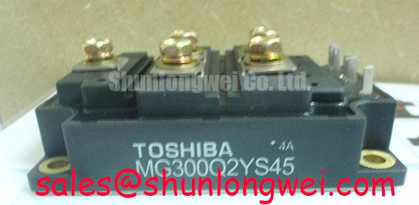
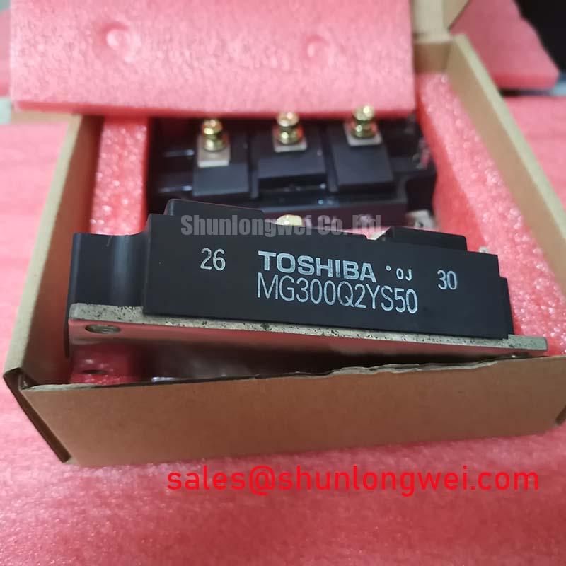
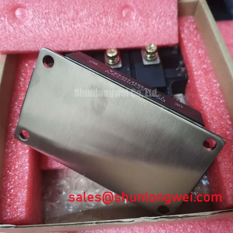
Before mounting MG300Q2YS50, inspect the mating heatsink for burrs, embedded debris, corrosion products, uneven coating residue, and evidence of previous overheating. Confirm that the module base and heatsink interface are clean and flat within the service requirements of the equipment. Apply the thermal interface material according to the equipment manufacturer’s assembly process, then tighten hardware in a controlled sequence using the specified bolt type and torque from the original mechanical documentation. Mounting torque, interface thickness, and fastening sequence are system assembly requirements unless explicitly stated by the module manufacturer.
Gate-driver return routing deserves the same attention as the power busbar. When an equipment design provides an auxiliary emitter return, it is commonly intended to give the driver a quieter reference point than the main high-current emitter path. Design Consideration: keep the gate-drive loop compact and keep its return separated from the path carrying major load-current transients until the connection point defined by the original design. This reduces mutual coupling that can otherwise alter the gate-emitter voltage seen by the semiconductor during switching.
During an emergency repair, technicians sometimes extend a damaged control lead with a longer wire or relocate its return to a nearby power terminal. That change can affect oscillation, turn-off behavior, and fault sensitivity even when the converter powers up normally at idle. Recreate the original lead routing, shielding arrangement where present, connector seating, and strain relief as closely as the equipment documentation allows. Then validate at controlled power with appropriate isolated measurement equipment.
Do not infer an auxiliary-emitter terminal from the module model name alone. The exact control-terminal assignment, polarity, and available terminals must be confirmed from the original Toshiba documentation and the host equipment’s wiring diagram. If the system does not provide a separately defined driver return, preserve the manufacturer’s intended gate-loop routing rather than creating a new connection scheme during service.
Assembly Integrity & Layout Architecture: Implementing High Frequency Commutation Loop Inductance for MG300Q2YS50
Inspect the DC-link capacitor connections, laminated or planar busbar joints, power-terminal hardware, and snubber network before energizing a repaired inverter leg. Loose joints, extended connection paths, damaged capacitor terminations, or altered busbar spacing can increase the commutation-loop inductance. During turn-off, the peak voltage is influenced by the DC-link voltage plus the inductive contribution associated with loop inductance and current-change rate. This Engineering Calculation relationship explains why a physically small interconnect change can produce a significant waveform change under load.
Design Consideration: minimize the physical area enclosed by the high-frequency commutation path to suppress inductive overshoot. The appropriate loop-inductance target, snubber-capacitor value, clamp arrangement, and switching rate must be determined by the converter’s original architecture and confirmed through measured peak voltage margins during switching tests. A component-level product page cannot prescribe those values because the result depends on busbar geometry, capacitor placement, switching frequency, gate-drive impedance, load current, and probe technique.
If excessive voltage ringing appears after module replacement, first verify that every power terminal is fully seated and tightened according to the equipment procedure, that the DC-link capacitors remain connected as designed, and that no busbar has been rotated or repositioned. Compare the affected phase with an intact phase where possible. A ringing difference may arise from layout asymmetry, a changed gate loop, degraded local decoupling, measurement-loop pickup, or an actual switching-stage defect. Capture collector-emitter voltage and gate-emitter voltage together so the time relationship can be assessed rather than judging the event from one waveform alone.
For MG300Q2YS50, retain the original clearance and creepage provisions established by the equipment designer, especially around DC-link conductors and control interfaces. The 1200 V official voltage rating is not a complete insulation-system specification for the finished inverter. Enclosure pollution level, altitude, busbar insulation, PCB construction, connector design, and applicable end-equipment standards must be evaluated by the system owner or qualified design authority.