
Content last revised on October 10, 2026
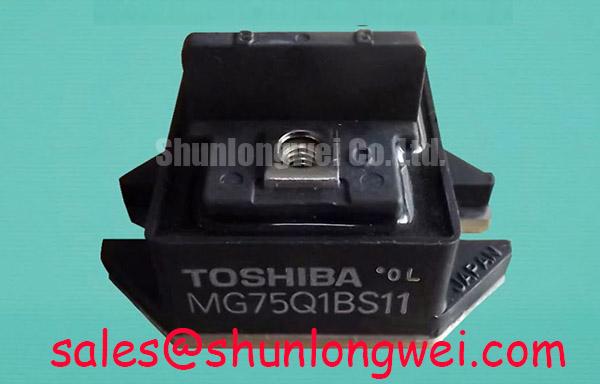
MG75Q1BS11 Toshiba 600V 75A IGBT Module
When a commercial inverter stops switching, isolate and discharge the DC link using the equipment manufacturer’s procedure and verify that it is de-energized. Record the original terminal wiring, and use a meter to check for unintended low resistance between the main power terminals before removing the Toshiba module. Confirm the nameplate and replacement documentation identify MG75Q1BS11, listed as a 600 V, 75 A IGBT module. These ratings do not establish allowable continuous operation without the applicable datasheet conditions. Mechanical fit, terminal arrangement, gate-drive compatibility, and heatsink contact must be checked against the failed assembly rather than assumed from current rating alone.
For commercial string inverter and microgrid energy storage repairs, the 600 V voltage class and 75 A current class provide the first procurement filter. They do not, by themselves, define switching frequency, allowable case temperature, short-circuit withstand, thermal impedance, or the correct gate-drive voltage. Those system limits belong to the applicable technical documentation and the converter design verification.
Field Diagnostics and Commissioning for Emitter Return Connections
Keep the power-current return path separate from any auxiliary emitter return used by the driver board. A high-current emitter trace can develop a transient voltage difference from the driver reference during rapid switching. If the control circuit senses that moving reference, the gate command may show ringing, delayed turn-off, or an apparent false trigger even when the module itself is electrically serviceable.
The listed product data identifies the device, voltage class, current class, and Toshiba module package, but it does not establish a Kelvin emitter terminal or a specific pin assignment. Before wiring MG75Q1BS11 into a replacement position, compare the original terminal map with the device documentation and the inverter schematic. Do not repurpose a power emitter terminal as an auxiliary driver return without confirming the internal connection.
On the bench, remove gate-drive power and discharge the DC link using the equipment manufacturer’s procedure. Photograph the busbar, gate wiring, and driver connector before loosening hardware. Then check continuity from each driver return point to the intended emitter reference and inspect whether the return conductor shares copper with the emitter load path. A shared path is a layout concern because the voltage developed by switching current can be injected directly into the gate-drive reference.
For a commercial string inverter or storage converter, the driver loop should remain compact, with the gate conductor and its return routed together and away from high-current commutation paths. Designers should minimize parasitic loop area and verify the result with an oscilloscope at the module terminals during controlled switching tests. A long motor cable or inverter output cable can behave as a transmission path, producing reflected voltage peaks that must be evaluated at the relevant cable terminals rather than inferred from the DC-link reading.
ROHM’s technical material on field-stop trench IGBTs and intelligent modules provides useful industry context for evaluating switching behavior and gate-drive interactions, but it is not a Toshiba specification for MG75Q1BS11. Use it as general semiconductor design reference only, alongside the original Toshiba documentation.
Thermal Interface Inspection and Inverter Replacement Fit
Thermal grease pump-out is commonly investigated through the complete mechanical stack: module baseplate, thermal interface material, heatsink surface, mounting hardware, and enclosure vibration. Inspect the baseplate for visible convexity, scoring, contamination, or local witness marks. Check the heatsink for burrs, debris, and uneven contact before installing the replacement module.
Uniform interface pressure matters because a thick region of thermal compound can increase the thermal path, while a dry or poorly covered region can create a local hot spot. A thin, continuous layer is a design consideration, not an MG75Q1BS11 factory specification. The compound type, application method, and final thickness should follow the interface-material manufacturer’s instructions and the equipment service procedure.
Use a calibrated torque tool and the documented tightening sequence so the baseplate settles evenly against the heatsink. The final torque is determined by the fastener size, module construction, heatsink design, and applicable mechanical documentation. Do not substitute a generic torque value for a Toshiba assembly instruction. After tightening, inspect the module for tilt, terminal stress, and movement before reconnecting the busbar.
Field Alert: Never tighten the mounting hardware against a contaminated or visibly uneven heatsink, because local pressure can damage the module baseplate or leave an ineffective thermal interface.
Gate interlock is a separate commissioning issue. In a half-bridge, both complementary switches must not receive overlapping turn-on commands. The dead-time buffer is system-determined and should be validated with the actual driver propagation delay, gate resistance, temperature range, and switching waveform. During first power-up, use a controlled current-limited test arrangement and confirm that both gate signals maintain the intended non-overlap under load.
The following comparison places the listed device beside another Toshiba reference model. The reference model’s specifications and compatibility require separate verification.
| Parameter | MG75Q1BS11 | MG75G1JL1 reference |
|---|---|---|
| Manufacturer | Toshiba | Toshiba |
| Category | IGBT Module | IGBT Module reference |
| Listed voltage rating | 600 V | Confirm from applicable documentation |
| Listed current rating | 75 A; verify applicable datasheet conditions | Confirm from applicable documentation |
| Package | Toshiba Module; verify dimensions and terminal layout | Confirm mechanical and terminal compatibility |
The MG75G1JL1 reference can support a neutral replacement review, but it should not be treated as a drop-in substitute until voltage, current, internal topology, terminal layout, gate characteristics, and mechanical dimensions match the equipment requirements.
Gate Loop Layout and High di/dt False Trigger Investigation
Separate the main load emitter connection from the auxiliary driver return wherever the verified module topology provides both paths. This prevents the gate loop from using the same conductor that carries the highest switching current. The objective is to reduce ground bounce at the driver reference and keep the gate-emitter voltage controlled during collector-current transitions.
Start at the module terminals and trace the gate cable back to the driver board. Look for long unpaired conductors, large routing loops, connector pins carrying both power and control returns, and parallel routing beside the busbar. These conditions can increase magnetic coupling. Re-route the gate signal and return as a close pair, keep the loop away from the commutation path, and use a controlled connector arrangement that preserves the intended reference.
Oscilloscope probing must be performed with a suitable differential or isolated measurement method. A long ground lead can create a measurement artifact that resembles gate ringing. Compare the gate-emitter waveform at the module with the signal at the driver output, then observe the collector-emitter voltage during the same event. If the waveform changes when the probe arrangement changes, correct the measurement method before changing hardware.
In a long-cable inverter installation, output-cable reflections can increase voltage peaks at the load terminals and couple noise into adjacent control wiring. Filtering and damping should be selected from measured waveform behavior, cable construction, load conditions, and switching timing. The system engineer should verify peak voltage and gate-emitter margins during commissioning rather than selecting a universal filter value.
The MG50Q1BS1 may be reviewed as another device reference, with its function and ratings checked against its own documentation. Its inclusion in a system discussion does not confirm electrical interchangeability with MG75Q1BS11. The rectifier stage, DC-link layout, switching bridge, and protection circuits must be assessed as one topology.
Protection Against dv/dt Cross-Conduction and Shoot-Through
High dv/dt can couple through the switching device capacitances and raise the inactive gate potential. If that transient exceeds the driver’s effective off-state control, the opposite switch may conduct briefly. The resulting cross-conduction is a system-level event influenced by gate resistance, driver impedance, layout inductance, common-emitter behavior, dead time, temperature, and the actual bus waveform.
A dedicated low-impedance turn-off path and an active Miller clamp are design considerations when the measured switching node produces unwanted gate movement. Their suitability depends on the driver architecture and the confirmed MG75Q1BS11 terminal arrangement. A negative off-bias may also be evaluated by the system designer where the driver and module documentation permit it, but the exact bias level must come from the validated gate-drive design rather than a generic prescription.
The practical test is to capture both complementary gate-emitter signals and the switching node during turn-on and turn-off. Check for overlap, delayed turn-off, excessive ringing, and a gate excursion on the inactive device. Repeat the measurement at relevant load and temperature conditions because a clean low-power waveform does not prove behavior at operating current.
Keep the gate driver supply decoupling close to the driver power pins, maintain a short return path, and avoid routing control traces across the high-current commutation loop. If an active clamp is used, confirm that its reference is connected to the correct emitter point. The article Evolution of Negative Off-Bias Gate Drive Circuits can be used as a practical reference when reviewing off-state gate-drive strategies.
For equipment evaluation, MG75Q1BS11 is identified as a Toshiba IGBT module with listed ratings of 600 V and 75 A, subject to the applicable datasheet conditions. Final commissioning should confirm terminal mapping, gate-drive behavior, thermal contact, interlock timing, and measured switching margins in the target commercial inverter or microgrid storage assembly.