

Content last revised on October 14, 2026
MG50Q1BS1 Inspection and Test Preparation
- With the equipment isolated and the DC link discharged, match the collector, emitter, and gate connections to the equipment schematic before attaching test leads.
- Record cold-state terminal measurements with the gate held at emitter potential, keeping instrument polarity and temperature consistent between comparisons.
- Inspect terminal seating, mounting surfaces, and the heatsink interface for contamination, uneven contact, or mechanical damage.
- Separate the gate driver and other connected electronics from the module before evaluating leakage or insulation with an approved test procedure.
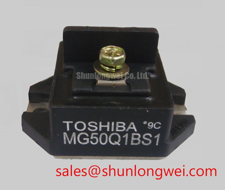
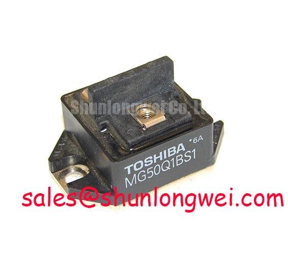
The MG50Q1BS1 is a Toshiba IGBT module with a 1200 V collector-emitter rating and a 50 A continuous collector-current rating at a case temperature of 25°C. Incoming inspection should distinguish simple connection checks from semiconductor parameter measurements: a handheld meter can reveal comparative conduction behavior, but it cannot establish rated-voltage leakage, saturation performance, or switching capability.
The following Official Specification values preserve their stated conditions. Terminal numbering, mechanical dimensions, tightening torque, and the complete switching-test circuit should be checked in the applicable Toshiba datasheet before fixture construction or replacement approval.
| Characteristic | Symbol | Condition | Official Specification |
|---|---|---|---|
| Collector-emitter voltage | VCES | Absolute rating | 1200 V |
| Gate-emitter voltage | VGES | Absolute rating | ±20 V |
| Continuous collector current | IC | Case temperature 25°C | 50 A |
| Pulsed collector current | ICP | Case temperature 25°C; pulse duration 1 ms | 100 A |
| Collector power dissipation | PC | Case temperature 25°C | 300 W |
| Isolation voltage | VISOL | AC; duration 1 minute | 2500 V |
| Collector-emitter saturation voltage | VCE(sat) | Collector current 50 A; gate-emitter voltage 15 V | 2.7 V maximum |
| Gate-emitter cut-off voltage | VGE(OFF) | Collector current 50 mA; collector-emitter voltage 5 V | 3.0 V minimum; 6.0 V maximum |
| Fall time | tf | Inductive load | 1.0 µs maximum |
| Collector cut-off current | ICES | Collector-emitter voltage 1200 V; gate-emitter voltage 0 V | 1.0 mA maximum |
For diode-mode inspection, establish the expected conduction path from the module circuit diagram rather than assuming an internal arrangement. Compare readings with a known-good unit under the same instrument conditions, and repeat measurements after controlled gate discharge. A changing reading can reflect stored gate charge or an external parallel path; it is not, by itself, a diagnosis of semiconductor damage.
💡 Bench Tip: Use ESD-controlled handling and discharge the gate through an appropriate protective path before comparing cold-state measurements.
Assembly Integrity & Layout Architecture: Implementing Transmission Line Impedance Mismatch: Sizi for MG50Q1BS1
Measure the inverter output and remote load-terminal waveforms separately when investigating spikes on long motor leads. As a Design Consideration, cable impedance and load impedance can produce reflected voltage steps when the switching edge travels along the cable. A remote-terminal peak is therefore not automatically the same event as collector-emitter overshoot at the MG50Q1BS1.
Use suitably rated differential probes, with connections arranged to minimize measurement-loop pickup. Preserve the operating condition while comparing traces: changing cable routing, load connection, or switching settings between captures can obscure the source of the disturbance. Record the DC-link voltage alongside the switching waveforms so that voltage stress can be assessed against the module’s 1200 V Official Specification without treating that absolute rating as an operating target.
A reflected step can reinforce the incident wave under severe impedance mismatch. The familiar idealized doubling applies to the incident traveling-wave step under particular boundary conditions, not to a guaranteed peak of twice the DC-link voltage in every installation. Actual terminal stress depends on cable losses, edge shape, termination, and successive reflections. This distinction matters when interpreting a remote motor trace alongside a local semiconductor trace.
Output filtering is a system-level Design Consideration. A dv/dt filter or output choke should be evaluated against cable characteristics, load current, switching frequency, and permitted voltage drop. Verify both remote-terminal edge behavior and local inverter switching stress after any filter change. A filter that improves the load-terminal waveform can also change current paths and resonances seen by the power stage.
At the module assembly, keep the commutation path compact and separate sensitive gate wiring from high-current conductors. Maintain insulation spacing through the terminal region, including the actual positions of busbars, washers, fasteners, and nearby grounded metal. Creepage and clearance are determined by the equipment’s insulation requirements and operating environment; the module’s isolation-test value does not prescribe a universal PCB spacing.
The 2500 V AC for 1 minute isolation rating is an Official Specification test condition, not a continuous working-voltage allowance or permission to repeat that test indiscriminately on an assembled converter. Insulation testing should follow the approved equipment procedure, with vulnerable driver circuits disconnected where required. Surface cleanliness, fixture leakage, and unintended connections must be resolved before attributing a result to the module itself.
Preventing Spurious Faults: PCB Symmetry Considerations for Dual IGBT Guidelines for MG50Q1BS1
Trace the gate-driver return to its physical emitter connection before changing gate resistance or protection settings. In a circuit using two IGBT switching positions, shared emitter-path inductance can couple power-current transitions into the gate reference. As a Design Consideration, separating the driver’s reference route from the main current route can reduce this coupling, but it does not establish that the MG50Q1BS1 contains a dedicated Kelvin-emitter terminal.
Where the verified terminal arrangement permits a separate external sense connection, take the driver return from the intended emitter reference point rather than a distant busbar location. Compare the complete gate loops on both switching positions, including connector routing and driver supply returns. Visual symmetry alone is insufficient: two neatly mirrored PCB traces can still have different electrical behavior when their power-current paths differ.
Observe gate-emitter voltage at the module connections during switching. A measurement taken only at the driver output can miss disturbances along the interconnect. Gate-loop damping should be tuned to suppress oscillation while retaining acceptable switching losses and protection response; the final resistance and drive arrangement are system-determined. Do not substitute an arbitrary damping value for waveform verification.
The ±20 V gate-emitter limit applies to positive and negative excursions. The 3.0–6.0 V cut-off-voltage specification is measured at a collector current of 50 mA and collector-emitter voltage of 5 V; it does not define a full-current drive command or an assured noise margin. For contextual gate-drive discussion, Evolution of Negative Off-Bias Gate Drive Circuits addresses off-state control approaches. Any implementation still requires validation against this module’s gate limits and the actual driver circuit.
Dead-time validation should include driver propagation differences, current decay, and temperature-dependent switching behavior. The Official Specification fall time of 1.0 µs maximum under an inductive load is not a complete dead-time prescription: it does not include every delay or current-tail contribution in the assembled converter. Evaluate both commutation directions and protection transitions, particularly where gate inhibition or restart logic changes the normal timing.
Fuse coordination also requires separate scrutiny. The 100 A for 1 ms pulsed-current rating at 25°C is not a fuse-clearing energy rating or proof of short-circuit withstand. Compare fuse let-through behavior with applicable semiconductor fault-withstand information and the protection circuit’s detection and shutdown behavior. A high-speed fuse can support fault containment without guaranteeing that an IGBT survives the initial fault interval.
For broader technology comparisons, ROHM Field Stop Trench IGBTs & Intelligent Modules and ROHM Silicon Carbide Power Devices & Modules provide manufacturer information about other power-semiconductor families. They are not specifications for the Toshiba MG50Q1BS1, and technology differences should not be translated into assumed pin compatibility or protection equivalence.
Benchtop Waveform Tuning: Mitigating Stress via Preventing Terminal Overheating via Period on MG50Q1BS1
Measure bolted-joint resistance with a four-wire instrument across the contact being evaluated, rather than including an uncontrolled length of busbar in the reading. As an Engineering Recommendation, keep the sense points and test-current path repeatable so that assembly comparisons remain meaningful. An acceptance threshold should come from the approved joint design or equipment service procedure, not an invented universal micro-ohm limit.
Before tightening a connection, check conductor flatness, terminal alignment, and the specified hardware stack. Mechanical preload should secure the electrical interface without distorting the terminal or transferring busbar strain into the module. Use the applicable tightening specification and inspect whether external conductors impose force after mounting. Increasing torque is not a reliable remedy for every elevated contact-resistance reading.
Thermographic inspection should compare corresponding joints under stable, recorded loading. Account for surface emissivity and reflected heat, especially on exposed metal. A local hot spot can arise from poor contact, uneven current distribution, adjacent heat sources, or restricted cooling; follow it with electrical and mechanical checks instead of assigning a single cause from the image alone.
The 50 A continuous-current and 300 W dissipation specifications both use a case temperature of 25°C. In equipment, the heatsink interface and cooling arrangement determine the case temperature actually reached. The specified 2.7 V maximum saturation voltage at 50 A and 15 V gate drive is useful for a controlled on-state test, but it does not include switching losses or every thermal condition encountered in operation.
Capture temperature behavior through load changes as well as steady operation. As a Design Consideration, reducing avoidable temperature excursions through appropriate cooling and operating control can reduce thermal-cycling stress, including in bidirectional charge-and-discharge stages. That principle does not support a numerical lifetime prediction for this module. Keep test records tied to case temperature, load, mounting condition, and cooling performance.
When evaluating compatibility for an industrial inverter welder or medium-frequency induction-heating power supply, compare the original circuit’s switching duty, gate-driver capability, cooling interface, and protection behavior. A cross-model review involving MG30G6EL2 should examine those same interfaces against each device’s own specifications; the model is not established here as a direct substitute.
After correcting a suspect connection, repeat the resistance measurement with the same fixture arrangement and repeat the thermal observation under comparable loading. Retain the before-and-after readings with the assembly record. This gives the next technician a reproducible basis for judging the joint without turning one successful bench run into an unsupported reliability claim.