




Content last revised on October 19, 2026
Assembly Integrity & Layout Architecture: Implementing Reverse Recovery Charge for MT506SV4CN
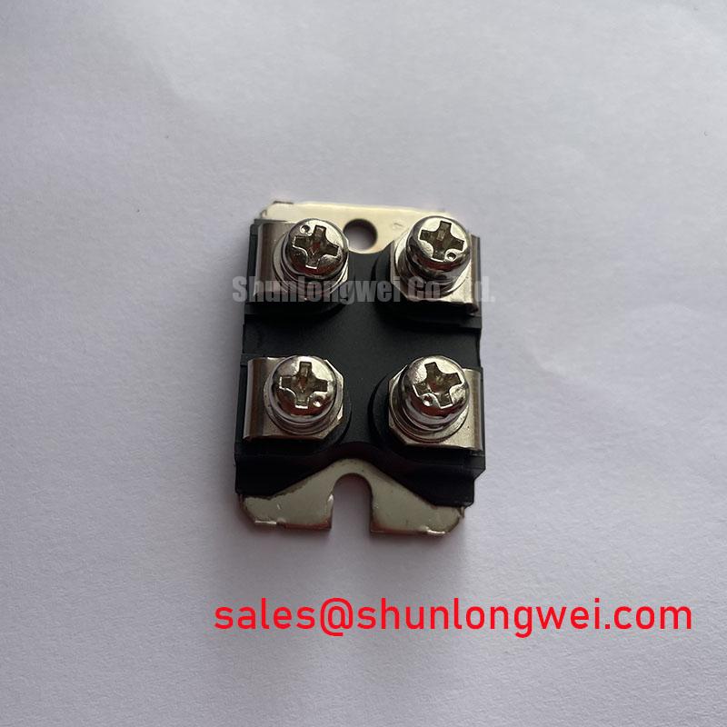
Start the service inspection by isolating the power stage, documenting each main terminal connection, and comparing the installed terminal arrangement with the replacement unit’s approved connection diagram. The MT506SV4CN is identified as a SanRex (Sansha Electric) thyristor power module for industrial power conversion assemblies. The exact circuit configuration, voltage and current ratings, terminal assignment, and thermal limits must be verified against the applicable manufacturer documentation.
Reverse recovery behavior deserves attention when this module is used in a commutation path. Reverse recovery peak current and recovery time influence turn off loss, voltage overshoot, and conducted or radiated interference. During troubleshooting, capture the commutation waveform at the actual power terminals rather than relying only on a controller fault code. A recovery waveform that differs from the known good phase may point toward busbar asymmetry, excessive stray inductance, or gate timing interaction.
Use the manufacturer’s fuse coordination guidance, where available, to compare the selected fuse clearing characteristic and total clearing I²t with the protected semiconductor path’s specified withstand limits. This comparison belongs to the complete protection design, not to the module name alone. Terminal lugs should be clean, flat, and mechanically supported so that tightening does not twist the power package or transfer cable strain into the terminals. Where a disc style pressure stack or double sided cooling arrangement is used elsewhere in the assembly, pressure uniformity should be checked across the complete stack according to its mechanical drawing.
Practical installation reminder: De energize, discharge stored energy, and verify the absence of hazardous voltage in the DC and AC sections before removing terminal hardware or reconnecting gate wiring.
For repair planning, the PDMB 200E6 is a separate product reference, not an established replacement for the MT506SV4CN. Electrical topology, ratings, mechanical envelope, gate characteristics, and protection requirements must be compared before considering any substitution.
Preventing Spurious Faults: Evaluating Post Surge Reverse Voltage Block Guidelines for MT506SV4CN
Post surge evaluation should begin with the surge waveform, duration, initial junction temperature, and reapplied voltage conditions stated in the relevant rating table, including the published ITSM value where applicable. The key field question is whether the junction temperature and cooling path permit operation within the specified limits when reverse voltage is reapplied. A surge event can damage the semiconductor, thermal interfaces, fuses, or insulation even when the control system has reset normally.
Record the event sequence from the SVC controller, inspect the fuse indicator and busbar joints, and compare the affected phase with an unaffected phase. The measurement plan should include phase current, reverse voltage, heat sink temperature, and the timing of the next firing command. The exact acceptance limits are determined by the manufacturer’s electrical and thermal tables together with the system protection study.
In a grid tied static Var compensator or thyristor switched capacitor bank, firing timing and symmetry influence reactive current and harmonic content; conduction angle control is commonly used in thyristor controlled reactor branches. A phase that fires late, misses a pulse, or receives an inconsistent gate command can produce an apparent overcurrent or voltage fault elsewhere in the cabinet. Oscilloscope probes should be connected with a measurement method suitable for the available common mode voltage, and the recorded waveform should be compared against the approved control sequence.
High voltage insulation coordination also depends on creepage, clearance, contamination, enclosure condition, and the construction of insulating barriers. Polyimide film is widely used as a high voltage dielectric insulation material in power assemblies; its presence in an assembly does not replace the system designer’s clearance and insulation verification. The general mechanism of avalanche stress is described in Avalanche Breakdown, but device level limits remain specific to the semiconductor and its operating conditions.
MT506SV4CN Circuit Protection & Reliability: Calibrating Gate Trigger Current Temperature Dependence
Gate trigger verification should focus on pulse amplitude, pulse width, rise behavior, repetition pattern, and timing relative to the anode to cathode voltage. The thyristor’s IGT and VGT characteristics are temperature dependent, so a firing circuit that appears stable during a cold inspection may behave differently after the cabinet reaches its normal thermal condition. Measure the gate pulse at the module terminals, not only at the driver output, because connector resistance, return path inductance, and routing can alter the delivered pulse.
For applications using a strong pulse train, the control engineer should verify that each pulse reaches the intended gate circuit and that any back porch gate current meets the firing design requirements. Anode current must reach the latching current before gate drive is removed and remain above the holding current for continued conduction. A gate current rise criterion above 1 A/µs may be used as a system engineering review point where specified by the firing design; it is not an MT506SV4CN factory rating unless explicitly listed in the applicable datasheet.
Minimize the loop area formed by the gate lead and its return path, keep high current commutation conductors physically separated from sensitive firing wiring, and verify the result under the highest expected switching disturbance. The firing board, isolation interface, pulse transformer if used, and module terminal arrangement should be assessed as one chain. Multi pulse firing can improve triggering consistency in some control architectures, but the pulse schedule must be validated against the controller’s synchronization and protection logic.
For wider application context, the Industrial Applications reference provides background on power semiconductor integration across demanding energy systems. When evaluating the MT506SV4CN for an SVC cabinet, final acceptance should be based on phase balance, surge response, gate waveform quality, thermal behavior, and documented protection coordination.