Content last revised on September 10, 2026
Incoming QA Checks for the NEC NL128102BC28-04 LCD Display
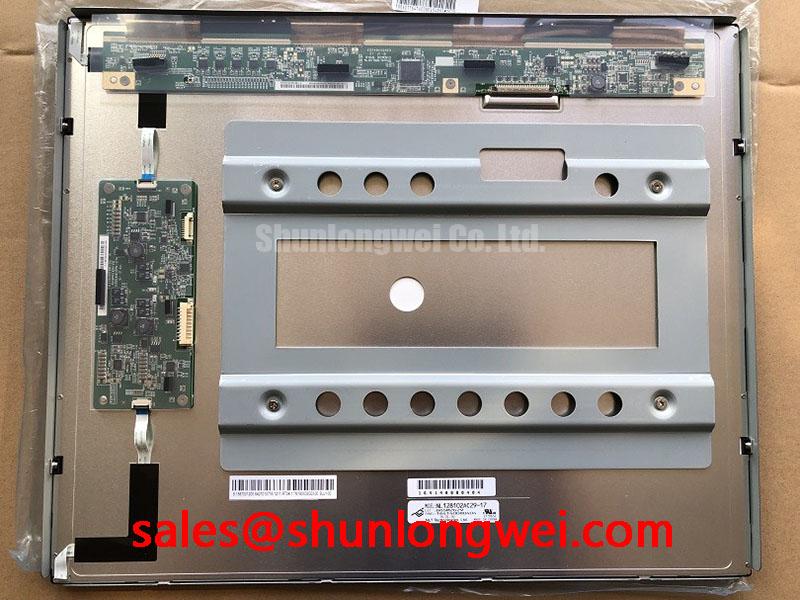
Start incoming inspection by checking the NEC NL128102BC28-04 identification, connector condition, glass surface, and visible display area before applying power. Use ESD protection, keep the panel on a clean, non abrasive surface, and compare the replacement unit with the original panel documentation before connecting any cable. The supplied product data identifies two optical configurations: a standard air gap assembly and an index matched optically bonded assembly. Confirm which construction is required for the equipment being repaired.
For optical inspection, the stated total interface reflectance is 8.0% to 9.5% at the air-to-polarizer boundary for the standard air gap assembly, while the index matched OCA configuration is specified at less than 1.5%. This difference is important when the display is evaluated in a bright control position, such as a marine radar or navigation bridge console. A panel that appears acceptable under indoor bench lighting may show reduced black level separation when exposed to direct ambient light.
The supplied contrast data records an effective contrast ratio of approximately 45:1 at 10,000 lux for the air gap configuration, with visibly washed out blacks. The index matched configuration is specified at more than 450:1 at 10,000 lux. At 50,000 lux, the stated effective contrast is below 12:1 for the air gap assembly and above 120:1 for the index matched configuration. These figures should be treated as assembly specific specifications, not as a general performance guarantee for every system installation.
Parallax is another incoming inspection point. The standard air gap assembly has a stated optical deviation of 1.1 mm to 1.8 mm, while the index matched assembly is specified at 0.0 mm optical offset. Check cursor alignment, radar overlay registration, and fine text positioning after installation, particularly where a touch overlay or protective front window is part of the equipment.
| Parameter | Stated product data | Practical verification |
|---|---|---|
| Optical assembly | Standard air gap or index matched optically bonded assembly | Compare the replacement construction with the original panel record |
| Interface reflectance | 8.0% to 9.5% air-to-polarizer boundary, or less than 1.5% with index matched OCA | Inspect under controlled light and the intended equipment viewing angle |
| Contrast at 10,000 lux | Approximately 45:1 or more than 450:1, depending on assembly | Use a calibrated luminance test arrangement where available |
| Contrast at 50,000 lux | Below 12:1 or above 120:1, depending on assembly | Evaluate legibility under the actual high light installation condition |
| Parallax deviation | 1.1 mm to 1.8 mm air gap, or 0.0 mm index matched assembly | Check graphical alignment against a known reference image |
Shielded FFC and LVDS Grounding at the Connector Interface
The NL128102BC28-04 signal data specifies a differential impedance of 100 Ω ±10%. This is an official product related target and should be considered together with the cable, connector, termination, and host T CON layout. A cable can meet a nominal impedance value while the assembled path still develops reflections through poor insertion, uneven contact pressure, an incorrect cable orientation, or an exposed shield transition.
For a replacement inspection, first examine the flexible cable for creases, contamination, lifted contacts, or an insertion depth different from the original installation. The FFC or FPC should enter squarely, with its contact face oriented according to the connector design. After locking the connector, inspect both sides for a uniform latch position. Do not use insertion force to compensate for a cable that is not aligned with the guide.
In an industrial cabinet containing variable frequency motor drives or servo equipment, a shielded LVDS path benefits from a continuous grounding strategy across the connector shell. This is a Design Consideration, not a specific NEC certification claim. The system designer should evaluate the 360 degree shield connection, chassis bonding, cable routing, and common mode noise control as one structure. Ferrite suppression may be evaluated where conducted or radiated interference is observed, but its material, placement, and impedance must be selected from system level measurements rather than assumed for this panel.
Pixel jitter, intermittent horizontal bands, or unstable grey transitions can have several possible sources. Inspect the connector seating first, then compare the differential waveform with a known good signal path. The stated intra-pair skew design rule is 50 ps or less, measured using active differential probing with deskew. The stated peak to peak clock jitter is less than 150 ps, assessed through real time phase jitter histogram analysis at the RxCLKIN differential input. These measurements require suitable probes and a controlled reference; they should not be inferred from a static continuity test.
Time domain reflectometry with a rise time below 35 ps is the listed bench method for evaluating the differential path. In practical repair work, access limitations may prevent a direct TDR measurement at the panel connector. In that case, inspect the complete cable route, verify connector retention, and use an oscilloscope with appropriate differential probing to compare clock quality, eye opening, and common mode behavior before changing the harness.
💡 Bench Tip: Disconnect power before inserting or removing the FFC or LVDS cable, and complete the final insertion with the cable held flat and parallel to the connector.
For a same class replacement evaluation, engineers may also compare the mechanical and electrical documentation of NL8048AC19-13KD, but connector arrangement, timing, optical construction, and host compatibility must be checked independently rather than assumed from display size or resolution.
Optical Luminance Evaluation and Backlight Retrofit Boundaries
Backlight diagnosis should begin with a controlled full screen test rather than a visual judgment from a single menu page. Display solid white, black, red, green, and blue images and inspect the centre, corners, and edge regions from the normal viewing position. Record visible luminance variation, dark zones, flicker, colour shifts, and any area that fails to illuminate. A 45 degree flashlight inspection can help reveal whether a dark appearance is associated with surface reflection, an inactive backlight region, or image data that is not being driven correctly.
The supplied data does not establish a universal backlight type, driver voltage, current, dimming method, service life, or failure rate for every NL128102BC28-04 assembly. The system integrator should verify the required backlight interface from the original panel documentation and the equipment wiring. Do not substitute a CCFL or LED driver solely because the replacement has the same visible dimensions. The driver output, connector pinout, enable logic, fault response, and thermal arrangement must all be compatible.
Some legacy display systems use high voltage CCFL ignition circuits, while modernized assemblies may use constant current LED drivers. Those are different integration paths, not interchangeable assumptions. If a retrofit is being considered, check the original enclosure clearance, cable insulation, electromagnetic noise, dimming control, and backlight fault reporting. A replacement driver should not be described as suitable until its output behavior has been tested with the actual panel assembly.
Luminance aging should be measured as a trend under the installed driver conditions. The supplied engineering brief refers to evaluation of an LED backlight decay curve toward 50% brightness at 50,000 hours, but no independent field dataset or laboratory life report is provided here. Therefore, a specific MTBF, half life guarantee, or brightness retention promise should not be assigned to this product page. For maintenance planning, record initial luminance, operating hours, ambient conditions, dimming state, and later measurements using the same test arrangement.
In a harsh marine radar or navigation bridge console, optical selection should account for sunlight, viewing angle, front window reflections, salt residue, and enclosure sealing. The stated index matched configuration has substantially lower interface reflectance and higher effective contrast under the supplied high illumination conditions. That does not independently establish an anti glare or anti reflection certification for the complete console. The front surface, protective window, cleaning method, and viewing geometry remain system responsibilities.
When investigating acoustic buzz or visible modulation, observe the backlight drive and the panel supply with suitable measurement equipment while changing brightness through the host control. A symptom may originate in the driver, wiring, control waveform, or panel interface. Verify the signal path and driver fault output before replacing the display. Any open circuit, short circuit, or overvoltage protection behavior must be confirmed from the original backlight documentation and the installed driver design.
Logic Supply Sequencing and Differential Display Timing
The host system should verify the required logic supply voltage from the original panel documentation before installation. The supplied integration brief references possible 3.3 V and 5.0 V system environments, but that reference does not authorize treating both values as interchangeable for this model. Apply only the documented voltage and sequencing required by the original display assembly and its controller.
Power sequencing should be checked with an oscilloscope at the panel connector while observing the enable, clock, data, and reset behavior of the host. A clean supply rise, a valid reset state, and correct signal arrival order help reduce abnormal startup images and intermittent initialization. The system designer must determine acceptable rise time and delay from the panel documentation and controller requirements; the values should not be invented from a general LVDS rule.
The differential interface should be routed as a controlled impedance path, with the stated target of 100 Ω ±10% used as the reference for the cable and board interconnect. Maintain pair symmetry, minimize unnecessary stubs, and avoid routing the display pair alongside noisy switching nodes where practical. These are Design Considerations for signal integrity, not a claim that the panel alone provides EMC compliance for the complete equipment.
JEIDA or VESA data mapping must be verified from the original timing documentation and controller configuration. Incorrect mapping can produce colour errors, split screen images, reversed pixel groups, or unstable grey levels even when the clock is present. Check the mapping configuration against a known good image and confirm the clock and data pairs individually when the symptom is intermittent.
At the T CON input, the supplied LVDS differential input voltage specification is 200 mV to 600 mV, measured by active differential probing at the input termination. The measurement location matters because a waveform measured at the source may not represent the amplitude or distortion at the panel connector. Compare the differential amplitude, common mode level, edge quality, and clock jitter at the receiving end where possible.
Grey scale and gamma evaluation should use stepped test patterns rather than photographic images. Look for missing levels, contouring, uneven transitions, or a channel that reaches black or white earlier than the others. These observations can involve timing configuration, T CON operation, gamma reference behavior, source data integrity, or panel damage. A panel page should not assign one cause without a controlled comparison.
Cold ambient operation also requires system validation. Liquid crystal response can change with temperature, and a visible grey to grey transition may become slower in a cold enclosure. If the equipment includes a heater, the system designer should verify heater control, warm up behavior, condensation management, and display timing under the intended environmental profile. No operating temperature range, heater rating, or cold response time is specified in the supplied product data for this page.
For broader background on panel interfaces, optical construction, and industrial TFT integration principles, refer to The Ultimate Guide to Industrial TFT LCD Technology. Use that material as general engineering context while treating the original NEC documentation as the controlling source for model specific installation limits.
Mechanical Stress Screening and Primary Colour Fault Isolation
Mechanical inspection should be completed before the panel is clamped into the equipment. Look for glass edge damage, uneven frame loading, connector displacement, and cable routing that could apply twisting force during insertion. The display should sit naturally in its mounting plane, with the enclosure designed to avoid point loading. Do not press the active area to correct an alignment problem caused by the chassis.
Micro twist or repeated cable movement may create intermittent faults that are difficult to reproduce during a short bench test. To separate mechanical sensitivity from signal or backlight behavior, display a white field and gently observe the image while checking the cable and frame without applying force to the glass. Any change should be documented and compared with the known good unit. Avoid flexing the substrate, pressing driver bond regions, or using a flashlight as a substitute for an electrical test.
A practical three stage colour check uses full screen white, black, and the primary colours red, green, and blue. White reveals broad luminance nonuniformity; black reveals light leakage and inactive regions; primary colours help identify channel specific data or driver abnormalities. Repeat the sequence after the panel reaches a stable operating condition, because startup behavior and backlight stabilization can otherwise be mistaken for a permanent display defect.
For dark shadow analysis, hold a flashlight at approximately 45 degrees to the front surface and inspect the affected region without touching the panel. This can reveal external reflections, surface contamination, or the boundary of a dark area, but it cannot by itself prove a driver bump or glass interconnect fracture. Confirm the finding with image pattern testing, cable substitution where appropriate, and comparison of the input waveform at the T CON.
Touch functionality, where present in the finished equipment, must also be tested as a system feature. The supplied data does not define a resistive or capacitive touch layer, glove sensitivity, water rejection, controller interface, or calibration specification for this model. The integrator should verify the original touch overlay and controller documentation rather than assuming that a visually matching LCD assembly supports the same touch behavior.
Finally, assess the complete front stack under the intended viewing light. The stated optical values distinguish the air gap and index matched assemblies, but they do not replace a system test of the bridge console window, anti glare treatment, anti reflection surface, cleaning chemicals, and enclosure geometry. Record the chosen assembly, connector condition, colour pattern results, luminance observations, and signal measurements in the incoming QA record before releasing the panel for field installation.