
Content last revised on July 15, 2026
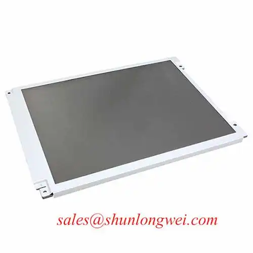
NL192108AC21-01 NLT 15.6" FHD Industrial LCD with SFT Technology
The NL192108AC21-01, manufactured by NLT Technologies (a Tianma group company), is a professional-grade 15.6-inch TFT-LCD module specifically engineered for high-precision visualization in medical and industrial environments. Delivering 1920x1080 Full HD resolution, it utilizes proprietary Super Fine TFT (SFT) technology to ensure color consistency across extreme viewing angles.
Key Specifications: 1920 x 1080 (FHD) | 400 cd/m² | 1000:1 Contrast Ratio
Core Engineering Benefits: Ultra-wide viewing angles (176°/176°) for multi-operator environments and a high-reliability LED backlight system designed for 50,000+ hours of continuous operation. One common question engineers ask is whether the backlight is replaceable for long-term maintenance; the NL192108AC21-01 confirms this capability, significantly lowering the total cost of ownership by allowing field-level servicing of the lighting unit rather than full module replacement. For medical diagnostic workstations requiring precise grayscale and wide viewing angles, the NL192108AC21-01 is the definitive choice.
Key Parameter Overview
Decoding the Specs for Enhanced Industrial Visualization
The following technical data is derived from the official manufacturer documentation to support engineering evaluation and system integration. Understanding the interplay between the 1000:1 contrast ratio and the LVDS interface is critical for achieving signal integrity in high-EMI environments.
Color Gamut72% NTSC (16.7M Colors)
| Optical & Display Characteristics | |
|---|---|
| Resolution | 1920 x 1080 (Full HD) |
| Luminance | 400 cd/m² (Typical) |
| Contrast Ratio | 1000:1 |
| Viewing Angle | 88°/88°/88°/88° (U/D/L/R) |
| Electrical & Interface Specifications | |
| Signal Interface | LVDS (2 ch, 8-bit) |
| Input Voltage | 3.3V DC (Typical) |
| Backlight Type | White LED (Replaceable) |
| Backlight Life | 50,000 Hours (Minimum to half brightness) |
| Mechanical & Environmental Data | |
| Active Area | 344.16 x 193.59 mm |
| Outline Dimensions | 363.8 x 215.9 x 6.3 mm |
| Operating Temperature | -20°C to +70°C |
| Storage Temperature | -20°C to +80°C |
Application Scenarios & Value
Achieving Precision and Reliability in High-Density HMI Designs
Industrial engineers often face the challenge of "parallax error" and "color wash-out" when operators view displays from non-perpendicular angles. The NL192108AC21-01 addresses this through its SFT (Super Fine TFT) technology, which is NLT’s high-end equivalent to IPS (In-Plane Switching). By aligning liquid crystals parallel to the glass substrate, it ensures that the 16.7 million colors remain accurate even at 88-degree off-axis viewing.
In high-end Medical Imaging and diagnostic equipment, the 1920x1080 resolution on a 15.6-inch canvas provides a pixel density that is ideal for reviewing detailed scans or complex patient data. The 400 nit brightness is specifically balanced for indoor clinical environments—bright enough for clarity under overhead surgical lights but calibrated to avoid operator eye fatigue during long shifts.
For industrial control rooms where 24/7 uptime is mandatory, the replaceable LED backlight is a strategic advantage. Unlike consumer-grade panels where a backlight failure necessitates replacing the entire assembly, the NL192108AC21-01 allows for modular repair. While this model is ideal for high-fidelity visualization, for applications where color accuracy is less critical than high-speed response, the related G156HTN02.1 offers a different performance profile based on TN technology. However, for Human-Machine Interfaces (HMI) in harsh environments, the -20 to +70°C operating range of the NLT module provides the necessary thermal headroom.
Industry Insights & Strategic Advantage
The Transition to Full HD Standards in Industrial Automation
The industrial display market is currently undergoing a significant shift from legacy XGA (1024x768) resolutions to Full HD (1920x1080) standards. This transition is driven by the increasing complexity of data visualization in Industrial IoT (IIoT) frameworks and the need for unified software interfaces that match the resolution of modern tablets and PCs. The NL192108AC21-01 acts as a bridge for this transition, offering the familiar LVDS interface while providing the high pixel density required for modern software dashboards.
To understand the technical depth of this display, consider an analogy: if a standard TN-type display is like a budget camera lens that gets blurry at the edges, SFT technology is like a high-end prime lens that maintains edge-to-edge sharpness and color neutrality. This is vital in safety-critical sectors like Railway Transit Control or Oil & Gas monitoring, where a misinterpreted color indicator on a screen could lead to operational errors. Furthermore, choosing industrial-grade displays over consumer versions significantly reduces the total cost of ownership by avoiding the frequent redesigns caused by the short lifecycles of consumer electronics.
Frequently Asked Questions
What are the primary advantages of SFT technology used in the NL192108AC21-01?
SFT (Super Fine TFT) is NLT’s proprietary technology that drastically improves viewing angles and color consistency. Unlike standard displays that suffer from color inversion when viewed from below, this 15.6-inch panel maintains a 1000:1 contrast ratio and consistent chromaticity from nearly any direction, which is essential for multi-operator monitoring stations.
How does the replaceable backlight feature impact long-term system maintenance?
Most industrial LCD failures are related to the backlight reaching its half-life. The NL192108AC21-01 is designed with a replaceable LED lamp power system. This allows maintenance teams to swap the lighting element without disturbing the TFT-LCD cell or the LVDS connections, extending the life of the medical HMI or industrial PC beyond the initial 50,000-hour rating.
Is the LVDS interface of this module compatible with standard industrial SBCs?
Yes, the 2-channel 8-bit LVDS interface is a standard in the industry, making the NL192108AC21-01 compatible with a wide range of industrial Single Board Computers (SBCs) and controllers. For detailed timing diagrams and pin assignments, engineers should refer to the LVDS interface standards to ensure optimal signal integrity over the 3.3V data lines.
For technical procurement and engineering support regarding high-resolution display integration, please consult our technical resources. We provide data-driven insights to help you navigate the complexities of TFT-LCD selection for your next mission-critical project.