Content last revised on September 16, 2026
PM15CTM060 Replacement Inspection and Initial Service Checks
Start a replacement inspection by isolating the drive, confirming the nameplate rating, and checking the PM15CTM060 terminals for abnormal cold resistance, carbonization, cracked molding, or loose mechanical hardware. The Mitsubishi Electric PM15CTM060 is an IPM rated at 600 V VCES and 15 A continuous collector current at TC = 25°C. These are official specification values and should be compared with the failed module, the DC link voltage, and the motor drive duty before any substitution is considered.
The module uses Mitsubishi Electric CSTBT™ carrier stored trench gate bipolar transistor technology. Its listed control supply voltage is 15 V, with a specified range of 13.5 V to 16.5 V. Integrated protection functions include over-temperature protection, short-circuit protection, and under-voltage lockout. These functions support practical troubleshooting, but they do not remove the need to verify control signals, current paths, cooling conditions, and switching transients at system level.
| Parameter | Official specification | Service significance |
|---|---|---|
| Collector emitter voltage | 600 V | Check the rating against the measured DC link and switching overshoot. |
| Continuous collector current | 15 A at TC = 25°C | Interpret current capability together with case temperature, switching frequency, duty cycle, and cooling. |
| Control supply voltage | 15 V, 13.5 V to 16.5 V | Measure the driver supply directly at the module interface during switching activity. |
| Switching technology | CSTBT™ | Supports a balance between conduction loss and switching behavior. |
| Integrated protection | OT, SC, UVLO | Protection status should be checked together with the controller fault history and control waveforms. |
PM15CTM060 Thermal Electrical Optimization: Galvanic Gate Drive Isolation and Practical Tuning
Begin the gate drive investigation with the power removed. Inspect the driver connector, isolation barrier area, gate return path, and control supply wiring before applying test power. A cold resistance check can identify a shorted power path or a damaged driver, but it cannot validate switching behavior. For a live test, use an isolated measurement setup and compare the high-side and low-side control-input waveforms with a known good channel from the same drive.
The PM15CTM060 control supply is specified at 15 V within the 13.5 V to 16.5 V range. The system integrator should verify that this voltage is present at the module pins under dynamic load rather than only at the driver power supply output. A supply that appears correct at idle may show disturbance during current commutation. The integrated under-voltage lockout should be treated as a protection function, not as a substitute for a stable gate drive supply.
Galvanic isolation is a system design consideration. Designers should verify the actual isolation rating, creepage, clearance, and common mode transient immunity from the applicable module and driver documentation. The supplied product parameters do not establish a reinforced isolation value above 5 kV or a CMTI value above 100 kV per microsecond for this specific unit. During validation, check whether the isolation barrier remains stable while the bridge switches against the intended DC link voltage. Unexpected switching pulses, repeated UVLO events, or unequal phase behavior require comparison of the isolation power supply, signal reference, and probe arrangement.
Keep the gate drive loop compact and separate it from the high current commutation path. The purpose is to reduce parasitic coupling and prevent the measured control waveform from being confused with a control command. Any gate resistance, damping network, or negative off bias must be selected by the system designer after checking the module data, driver output capability, switching loss, and turn off margin. A typical starting point may be evaluated on the bench, but it should not be treated as an official PM15CTM060 setting.
Mitsubishi Electric describes CSTBT technology in its power semiconductor application material. Engineers assessing switching loss and motor control behavior can review the manufacturer information on Mitsubishi Electric CSTBT™ Technology. The switching result still depends on the complete inverter layout, gate driver, motor cable, load profile, and thermal path.
Benchtop Waveform Tuning: Dynamic Braking Chopper Operation with PM15CTM060
When a robotic articulator or small automation axis decelerates, its motor can return energy to the DC link. The service engineer should first determine whether the drive uses an internal braking function or an external chopper and resistor assembly. Confirm the DC link trend during commanded deceleration, then compare the measured voltage with the system capacitor rating and the documented protection threshold. The PM15CTM060 voltage rating alone does not define the permitted braking profile.
Braking resistor selection is a system calculation based on regenerated energy, deceleration time, repetition rate, resistor pulse capability, enclosure temperature, and the chopper switching duty. The IGBT current rating must be evaluated together with conduction loss and switching loss. If a resistor is replaced with a different value or physical construction, the control parameters and thermal behavior require renewed verification. Do not infer resistor suitability from resistance value alone.
For a suspected braking fault, inspect the chopper terminals for discoloration, measure the resistor path with the DC link fully discharged, and verify the control command at the chopper module interface. A missing control command, an intermittent over-voltage trip, and excessive resistor temperature can have different causes, including control timing, sensing error, wiring damage, or insufficient heat transfer. Use an oscilloscope and the drive service documentation to correlate the command, DC link voltage, and chopper current.
Thermal interface material should cover the intended contact surface evenly without contaminating insulation distances. The supplied product information does not specify a PM15CTM060 TIM thickness or a mounting torque. A thin, uniform application is a general design consideration, while the correct fastener torque and tightening sequence must follow the heatsink, screw, washer, and assembly documentation. A cross pattern can help distribute mounting pressure, but it does not establish a product specific torque value.
Field Alert: Disconnect the DC link, wait for the documented discharge interval, and verify the voltage with an appropriate meter before touching the module or braking circuit.
After reassembly, inspect the heatsink contact, insulation hardware, and terminal clamping before the first powered test. Run the axis at a controlled load and observe the case temperature, DC link behavior, fault output, and braking waveform. The evaluation should continue until the worst expected deceleration and repetition pattern has been tested under the actual enclosure and airflow conditions.
PM15CTM060 Operational Boundaries: Evaluating High Frequency Common Mode Bearing Current
Long motor cables can produce ringing and common mode current when their characteristic impedance interacts with the inverter output and motor input. The resulting terminal voltage can exceed the steady DC link level during switching. A specific two times VDC spike should not be assumed for every PM15CTM060 installation because the result depends on cable length, termination, motor construction, switching edge rate, grounding, and measurement technique.
For field troubleshooting, inspect the motor cable shield termination, protective earth bonding, output terminals, and bearing insulation arrangement where applicable. Capture the phase to phase and phase to earth waveforms with a suitable differential probe. Compare the waveforms at the inverter and motor ends when the cable length or routing is suspected of contributing to ringing. A waveform that changes substantially with probe placement may indicate a measurement loop problem rather than a module fault.
Output chokes, dv/dt filters, sine filters, and common mode components should be evaluated according to the motor insulation system, cable construction, drive switching frequency, allowable voltage rise, and thermal losses. The PM15CTM060 official parameters provided here do not specify a filter value, cable length, bearing current limit, or permitted dv/dt. Designers should therefore select the filter from the complete drive design and verify the semiconductor voltage margin during switching tests.
Common mode current may also disturb encoder feedback, safety circuits, or isolated communications. Separate power and signal routing where practical, maintain the required insulation distances, and check the grounding topology against the original machine design. If a fault appears only with the motor connected, compare the control command and output waveform with the motor disconnected under an approved service procedure. This helps separate control instability from load and cable interaction without assigning a single cause prematurely.
Silicon carbide modules can be considered as a separate technology option where higher switching frequency or lower switching loss is required, but their gate drive, insulation, layout, protection, and electromagnetic behavior are different. Product comparisons should be made from the complete application requirements. Reference information is available from Wolfspeed Silicon Carbide power modules.
PM15CTM060 Circuit Protection and Reliability: Calibrating PCB Gate Loop Symmetry
Inspect the PCB gate loop for unequal trace length, narrow necks, unnecessary vias, shared return paths, and coupling with the collector or emitter power copper. The high current emitter return and the control reference should be routed according to the module pin definition and driver design. Where an auxiliary control emitter connection is provided, keep its return function distinct from the main commutation path so that load current does not create an unwanted control reference shift.
Gate loop symmetry matters when several switching paths share a board. A phase that switches differently from the others may reflect layout imbalance, driver supply disturbance, a damaged isolation channel, or unequal parasitic inductance. Compare the control-input waveforms at the module interface, not only at the driver output. Verify switching turn-off behavior, fault response, and the relationship between the protection signal and the actual collector current.
The PM15CTM060 includes short circuit and over temperature protection, but protection response is still influenced by wiring, sensing, controller timing, temperature, and the external gate drive. Do not use the presence of SC or OT protection as evidence that every short circuit or overload condition is safe. The system designer must verify the protection sequence and energy involved under the intended fault conditions.
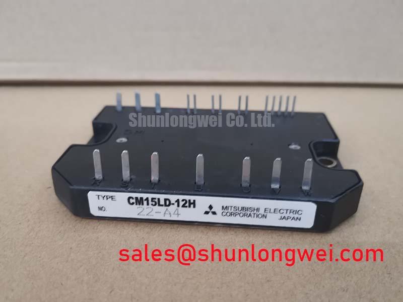
For maintenance, record the original connector orientation, terminal markings, heatsink arrangement, and control wiring before removal. Check the replacement against the required voltage, current, control supply, protection interface, mechanical fit, and thermal interface. The CM100DY-12E may be evaluated as a separate candidate device only after the engineer confirms electrical, mechanical, thermal, and control compatibility from the relevant documentation.
When switching turn-off behavior remains unstable, the technical background in Evolution of Negative Off Bias Gate Drive Circuits can help frame the role of off-state gate control and parasitic coupling. Any negative gate bias, active clamp, or damping network must be validated against the actual module interface requirements and driver insulation design; it should not be assumed to be applicable to the PM15CTM060. Final acceptance should be based on measured control-input waveform, collector-emitter overshoot, thermal response, fault behavior, and the required motor control duty.