

Content last revised on October 9, 2026
Preventing Spurious Faults: Auxiliary Emitter Return Trace Separation Guidelines for QM100TX1-HB
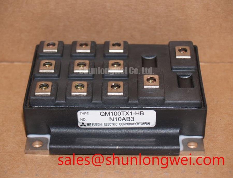
With the equipment isolated and its DC link verified discharged, compare the QM100TX1-HB terminal markings with the original circuit diagram before taking cold resistance or diode-mode readings. Record probe polarity, terminal pair, and module temperature so that subsequent measurements remain comparable. A reading taken through the connected driver, snubber, or motor circuit is not an isolated measurement of the module.
The Mitsubishi Electric QM100TX1-HB is an Isolated Darlington Module, not an insulated-gate IGBT module. It is a 600 V, 100 A device; the current rating must be interpreted under the manufacturer's specified conditions, not as an unconditional operating current. This distinction matters during repair: base-drive current, collector-emitter behavior, and switching charge removal require different checks from those used for an IGBT gate circuit. The model name alone should not be used to infer a different current rating.
| Product characteristic | Specified value | Engineering interpretation |
|---|---|---|
| Model | QM100TX1-HB | Match the complete designation against the equipment documentation. |
| Manufacturer | Mitsubishi Electric | Use the corresponding manufacturer terminal drawing for connection checks. |
| Rated voltage | 600 V | Not a recommended DC-link operating voltage or a package isolation-test voltage. |
| Rated collector current | 100 A under the manufacturer's specified conditions | Operating suitability also depends on the applicable thermal and switching conditions. |
| Package classification | Isolated Darlington Module | Does not independently establish an insulation withstand value or test procedure. |
Start return-path assessment at the terminal drawing rather than assuming that the QM100TX1-HB provides a dedicated auxiliary or Kelvin emitter. A separate emitter connection is not established by the specifications above. Identify the documented base, collector, and emitter connections, then trace how the equipment routes the driver return and load current. If the original assembly uses additional return wiring, establish its actual connection point before reproducing it.
As a Design Consideration, shared impedance between a driver return and a high-current emitter path can disturb the voltage seen by the drive circuit during switching. The practical objective is to keep control-current routing from unnecessarily sharing load-current paths. Any separation must preserve the original circuit reference and follow the documented terminal arrangement; adding an assumed emitter connection is not a valid repair method.
Inspect connectors, solder joints, bus connections, and driver-board return tracks before attributing intermittent trips to the semiconductor. With power removed, compare continuity and contact condition against a known-good assembly of the same configuration. During controlled commissioning, a qualified technician can compare the driver-side signal with the signal at the module terminals using appropriately rated differential measurement equipment. Differences that coincide with load-current transitions warrant investigation of the return path and measurement setup.
Diode-mode testing should likewise follow documented junction paths. A Darlington assembly cannot be judged by a universal single-junction forward-voltage threshold, and surrounding resistors or diodes can alter a meter reading. Record both probe orientations and distinguish a stable reading from a charging transient. An unexpected result is a reason to isolate the relevant circuit branch and repeat the measurement, not sufficient evidence for a single-cause diagnosis.
💡 Bench Tip: Apply appropriate ESD precautions and compare cold readings with an electrically isolated, known-good module of the same designation before interpreting a polarity-dependent reading as a fault.
For repair purchasing, the QM200HA-HK can be included in a separate specification comparison, but its listing does not establish interchangeability with QM100TX1-HB. Terminal arrangement, transistor configuration, drive requirements, switching characteristics, and mechanical fit must all be checked before an engineering team approves any substitution.
Field Diagnostics & Commissioning: Overvoltage Trip Prevention via Switching Transient Control in QM100TX1-HB Topologies
When evaluating this module in a heavy-duty variable-frequency AC motor drive, first determine whether an overvoltage trip originates from a rising DC link or a local switching transient. These are different measurements and can require different corrective actions. Capture the DC-link behavior alongside the relevant collector-emitter waveform under a controlled operating condition, using probes whose voltage rating, common-mode performance, and connection method suit the circuit.
The 600 V rating is not permission to operate the DC link at that voltage. As a Design Consideration, the system engineer should assess the measured collector-emitter peak, switching conditions, temperature, and the manufacturer's applicable operating limits together. A voltage trace taken at a distant bus connection can miss a local transient at the module, while an unsuitable probe connection can introduce apparent ringing.
During motor deceleration, regenerated energy can raise the DC-link voltage if the equipment cannot return or dissipate that energy adequately. Check the original braking circuit, resistor connections, control enable conditions, and protective devices. The QM100TX1-HB specifications listed here do not establish an internal braking switch, resistor capacity, or braking duty. Any external braking transistor and resistor should be evaluated from the machine's energy profile, repetition rate, thermal limits, and controller behavior rather than selected from this module's current rating alone.
As a Design Consideration, diode recovery and parasitic circuit inductance can contribute to switching overshoot and ringing. Establish the actual freewheeling path from the equipment schematic before examining the relevant waveform. Inspect existing snubber connections and components against the original design. Changes intended to reduce ringing also affect dissipation and switching behavior, so their suitability should be verified under the system's operating conditions rather than inferred from a cleaner unloaded trace.
When mapping the complete power stage, documentation for the QM100HY-2H may be reviewed separately if that device appears in an associated assembly. It should not be assigned a rectifier, braking, or complementary-switch role without confirming its circuit configuration and the equipment schematic. Similar product names do not establish a shared topology.
The manufacturer's Mitsubishi Electric SiC Power Modules & SBDs material concerns a different device technology; it is not a source of QM100TX1-HB switching limits. Measurements on this Darlington stage should be assessed against its own documentation. Reducing observed ringing also does not establish whole-equipment EMC compliance.
Preventing Spurious Faults: Output Sinusoidal Filter vs dv/dt Reactor Guidelines for QM100TX1-HB
Before associating a drive trip with the module, inspect the motor cable, output connections, grounding arrangement, and any installed output filter. Cable replacement or rerouting can change the load presented to an existing inverter even when the motor itself is unchanged. Document the installed cable arrangement and compare it with the equipment manufacturer's permitted configuration.
As a Design Consideration, a sufficiently long motor cable behaves as a transmission line during fast voltage transitions. Reflections depend on cable characteristics, termination impedance, and the relationship between propagation time and switching-edge duration. The motor-terminal waveform can therefore differ from the inverter-terminal waveform. A fixed multiplication factor should not be treated as a guaranteed property of a QM100TX1-HB installation; measure the relevant endpoints under representative conditions.
A dv/dt reactor or filter principally addresses the transition presented to the cable and motor, whereas a sinusoidal output filter targets stronger attenuation of switching-frequency content. Neither is automatically compatible with an existing drive. Designers should verify switching behavior, output frequency range, filter losses, resonance, controller interaction, and the motor manufacturer's insulation requirements before changing the output network.
For troubleshooting, compare inverter-side and motor-side voltage traces with suitable differential instrumentation. Inspect filter connections and look for changes in behavior with cable configuration or operating condition. An abnormal waveform may reflect several interacting causes, including the output network or measurement arrangement; it does not by itself establish semiconductor damage. Preserve the original protection functions during testing.
The Clarke transformation used in motor-drive analysis describes how phase quantities can be represented for control calculations. It does not determine cable reflection amplitude, module terminal assignments, or output-filter compatibility. Keeping control mathematics separate from hardware acceptance criteria helps prevent a functioning control algorithm from being mistaken for proof of a safe power-stage integration.
For electrical-clearance and insulation review, consult the equipment's documented requirements and applicable installation standards. The Field Engineer’s Handbook offers supplementary testing and failure-analysis context, but does not replace the module's specified limits. In particular, do not derive a package withstand-test voltage from the 600 V transistor rating.
Preventing Spurious Faults: Negative Gate Bias vs Active Miller Clamping Guidelines for QM100TX1-HB
The first compatibility check here is terminology: QM100TX1-HB is a Darlington module, so an IGBT negative-gate-bias or active-Miller-clamp prescription cannot be transferred directly to it. Its control connection is a base, not an insulated gate. Establish the original base-drive circuit and the manufacturer's permitted base-emitter conditions before making changes intended to improve turn-off behavior.
As a Design Consideration, bipolar transistor switching depends on drive current and stored-charge removal. Examine the driver supply, output stage, base-current path, and return connection when investigating delayed turn-off or unintended conduction. A driver intended for an insulated-gate device is not automatically a suitable replacement, even if its output waveform appears similar at first inspection.
During commissioning, compare commanded switching with the measured base-emitter and collector-emitter behavior using the original equipment's approved procedure. Where the circuit contains opposing switches, investigate their timing and conduction behavior together. Unexpected current can have multiple contributors, including drive-path defects, charge-removal behavior, and load conditions. A static meter check cannot establish satisfactory dynamic turn-off.
Negative base-emitter drive, where explicitly supported by the original design, must remain within the manufacturer's documented limits. No universal bias voltage, clamp circuit, or timing value follows from the voltage and current ratings given here. Before returning the assembly to service, verify the documented drive arrangement, thermal interface, terminal fastening requirements, and protection response under controlled conditions appropriate to the equipment.