
Content last revised on September 25, 2026
PS11036-Y2 Thermal Electrical Optimization: Overvoltage Trip Prevention Through Fast Switching Practical Tuning
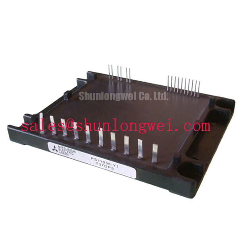
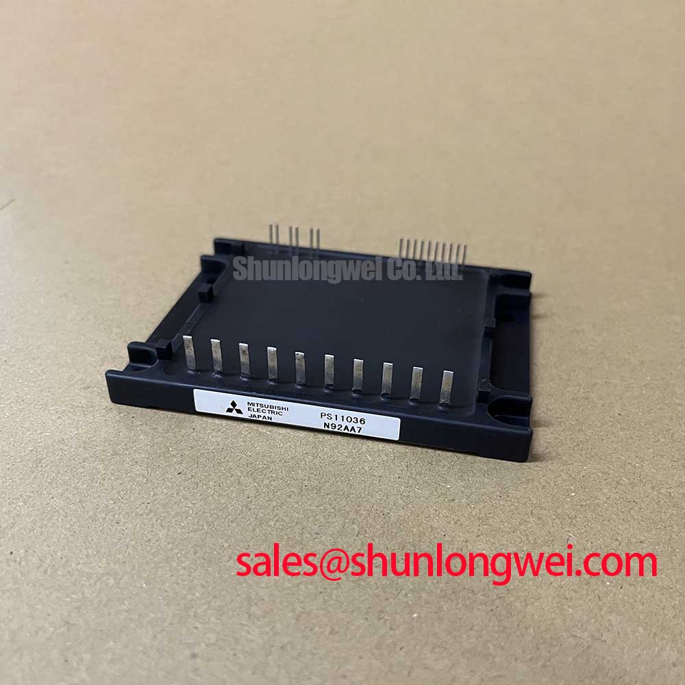
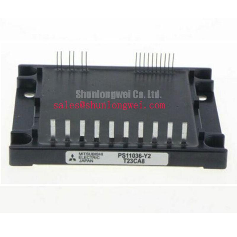
Before energizing a replacement unit, verify the marking, inspect the Mini DIPIPM package for cracks or bent terminals, and compare the cold resistance pattern between corresponding power terminals and a known good reference. The PS11036-Y2 is a Mitsubishi Electric DIP-IPM with an official rated voltage of 600 V and an official rated current of 15.0 A. These ratings identify the device category and electrical boundary, but they do not replace system-level checks for switching surge, thermal loading, motor current, or braking energy.
For light industrial automation and multi-joint robotic articulators, the DC link can rise during rapid motor deceleration. Designers should evaluate the braking path, ballast resistor, DC-link capacitance, and protection threshold together. A braking IGBT or external braking stage must be selected from the measured kinetic energy, duty cycle, resistor pulse capability, and allowable DC-link voltage. The PS11036-Y2 rating should be treated as an official component specification, while the correct braking arrangement remains a system engineering decision.
Fast switching reduces conduction and switching losses in some operating conditions, but excessive loop inductance can create voltage overshoot during turn-off. Keep the high-current commutation path compact, arrange the DC-link capacitor close to the power terminals, and verify the actual collector-emitter waveform with a properly rated differential probe. An overvoltage event should be investigated against bus voltage, switching speed, gate-drive behavior, motor regeneration, and measurement setup rather than assigned to one cause.
When comparing compatible industrial power-module families, engineers may also review the electrical and mechanical documentation for 7MBR15SA120. It should be treated as a separate device for formal pin, control, thermal, and ratings verification. Do not assume interchangeability from current and voltage markings alone.
| Parameter | PS11036-Y2 information | Engineering use |
|---|---|---|
| Manufacturer | Mitsubishi Electric | Confirm the original equipment documentation and approved assembly drawing |
| Package | DIP-IPM / Mini DIPIPM | Check footprint, terminal assignment, isolation spacing, and mounting constraints |
| Rated voltage | 600 V, Official Specification | Compare with DC-link voltage and measured switching overshoot |
| Rated current | 15.0 A, Official Specification | Compare with motor current, overload duration, modulation, and cooling conditions |
PS11036-Y2 Circuit Protection and Reliability: Calibrating SCSOA Overcurrent Protection
Static verification should begin with the original equipment pinout and the manufacturer’s application documentation. Identify the power terminals, control terminals, supply references, and fault output connections from the correct drawing before applying any external signal. A multimeter diode test can help compare the forward conduction path of the power devices, but the reading is only a comparative cold-state check. It is not proof that the gate insulation, internal driver, short-circuit protection, or temperature-sensing functions are healthy.
The requested short-circuit safe operating area and detection timing must be confirmed from the applicable Mitsubishi Electric documentation for the exact revision. A value such as detection within 10 microseconds should not be treated as an automatic PS11036-Y2 specification without that source. As a Design Consideration, the protection chain should detect abnormal VCE behavior, prevent uncontrolled gate drive, and manage the turn-off transition so that the resulting inductive voltage remains within the verified system boundary.
Two-stage soft turn-off is commonly evaluated when an abrupt gate command would produce excessive di/dt. The actual gate resistance, blanking behavior, fault latch logic, and control voltage must be determined from the module documentation and the host inverter design. During bench testing, use a current-limited, isolated setup and record the fault signal, gate waveform, collector-emitter voltage, and DC-link response on the same time base.
Creepage and clearance must be checked on the complete assembly, including the PCB, busbar, contamination environment, coating, connector geometry, and enclosure. The module’s 600 V rating does not independently certify the finished inverter for insulation coordination or safety compliance. Busbar fasteners should be secured according to the equipment manufacturer’s mechanical procedure, with attention to vibration, conductor movement, terminal stress, and thermal expansion.
Bench Tip: Protect the device against ESD, discharge the DC link before every connection change, and compare diode-test results with a documented cold-state reference rather than relying on one absolute meter value.
For gate-drive noise and off-state control behavior, the technical discussion in Evolution of Negative Off-Bias Gate Drive Circuits provides useful background. Any negative off-bias voltage, common-mode filtering, or gate clamp arrangement must still be verified against the PS11036-Y2 control interface documentation. Designers should examine ground bounce and probe reference errors before changing gate-drive values.
PS11036-Y2 Transient Dynamics and Electrical Design: Planar Symmetrical Busbar Geometry
During a switching test, the measured peak voltage is influenced by DC-link voltage, commutation inductance, current slope, probe loop area, and the physical location of the measurement point. The familiar relationship between peak voltage, DC voltage, stray inductance, and di/dt is useful as an Engineering Calculation, but it should be applied with measured waveforms rather than used to assign an unverified inductance target to this module.
A practical layout review should trace the complete high-current loop from the DC-link capacitor through the PS11036-Y2 power terminals and back to the capacitor. Minimize loop area, avoid unnecessary conductor overlap, and keep positive and negative paths physically balanced where the mechanical design permits. A planar symmetrical busbar can reduce magnetic imbalance, but the final result depends on copper geometry, terminal arrangement, capacitor construction, fastener spacing, and current distribution.
Snubber selection is a Design Consideration requiring oscilloscope evidence. The capacitor, damping resistance, parasitic inductance, pulse current, dielectric behavior, and repetitive dissipation must be evaluated as one network. A snubber that suppresses one switching edge may increase loss or alter the gate and commutation waveform elsewhere. Validate the change at the intended DC-link voltage, motor current, switching frequency, and thermal condition.
The Mitsubishi Electric Power Semiconductors and High-Power Modules resource is an appropriate reference point for manufacturer terminology and power-device application context. For comparison with other integrated power-module architectures, engineers can consult Infineon’s CIPOS Intelligent Power Modules information. Neither external family information should be used to infer unlisted PS11036-Y2 pin functions or limits.
PS11036-Y2 Assembly Integrity and Layout Architecture: Dynamic Power Loss Dissipation
Thermal verification should use the actual switching waveform, load profile, cooling assembly, and enclosure conditions. The official 15.0 A current rating cannot by itself predict junction temperature during robotic-axis acceleration, deceleration, stall, or repeated positioning. Designers should separate conduction loss, switching loss, diode recovery behavior, driver consumption, and braking-stage dissipation before estimating the thermal margin.
For pulsed overload analysis, a transient thermal impedance network can represent the junction-to-case response as several time-dependent thermal paths. This is an Engineering Calculation, not an additional PS11036-Y2 datasheet value. The correct Zth curve, case reference, pulse duration, duty cycle, and mounting interface must come from the applicable technical documentation. Peak junction temperature should then be checked against the documented operating limits under the worst credible pulse sequence.
Use a clean, controlled thermal interface and ensure that the module sits squarely against its specified heat-spreading surface. Check mounting flatness, fastener sequence, connector clearance, and airflow obstruction during assembly inspection. Thermal imaging can locate uneven heating, but it does not directly measure semiconductor junction temperature; correlate it with electrical loss calculations and temperature-sensing data where available.
When a field unit trips after repeated motion, record the DC-link voltage, phase current, fault timing, heat-sink temperature, switching frequency, and ambient condition. Inspect solder joints, terminal pressure, busbar movement, and cooling-path contamination. The combination of electrical records and physical inspection is more reliable than replacing the PS11036-Y2 repeatedly without identifying whether the initiating stress came from regeneration, protection timing, commutation overshoot, or thermal accumulation.