

Content last revised on October 25, 2026
Assembly Integrity & Layout Architecture: Implementing Transient Thermal Impedance for QM150DY-24BK
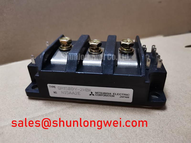
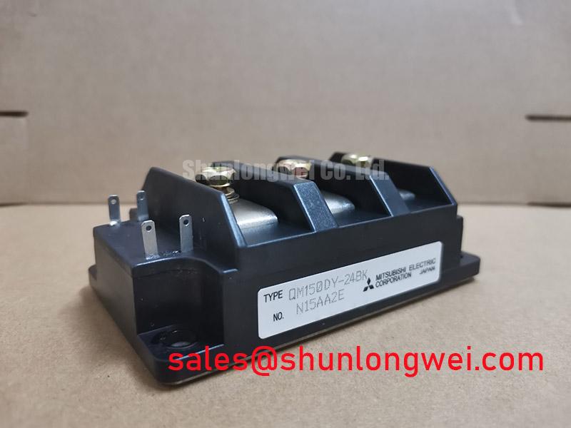
Transient thermal impedance must be treated as a time-dependent junction-to-case path when the QM150DY-24BK experiences pulsed current, repeated acceleration, or short overload events. A single steady-state thermal-resistance value cannot describe the temperature response of a short pulse. The practical model uses several thermal resistance and capacitance sections, with each section representing a different heating and cooling time constant between the semiconductor junction and the case.
For an engineering calculation, the load profile is divided into pulse intervals and the temperature rise is evaluated by superimposing the relevant transient thermal impedance response for each interval. The resulting peak junction temperature is then compared with the applicable device limit and the system derating policy. The model should include pulse width, duty ratio, repetition pattern, case temperature, and the actual cooling path rather than relying on the nominal 150.0 A rating as a thermal guarantee.
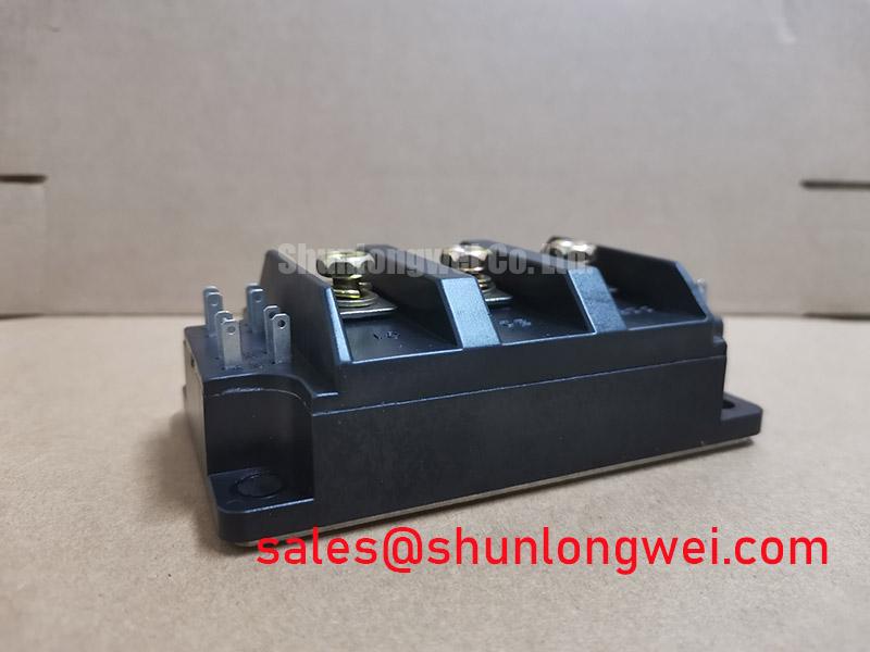
The mechanical stack deserves the same attention as the electrical model. The baseplate and heatsink faces should be clean, flat, and free from particles that can create a local air gap. Thermal interface material should be applied as a uniform, controlled film according to the interface supplier and module assembly instructions. Excess compound can migrate toward nearby insulation surfaces, while insufficient coverage can leave dry regions that raise the local case temperature.
Fasten the module progressively and evenly so that the baseplate does not tilt during compression. The correct bolt type, washer arrangement, torque sequence, and final torque must come from the relevant mechanical documentation; a generic torque value should not be treated as an official QM150DY-24BK parameter. After assembly, inspect the heatsink contact pattern and use thermography during a controlled operating test to locate abnormal temperature gradients across the power path.
Layout architecture should keep the commutation loop compact and prevent high-current paths from crossing sensitive control wiring. Minimize stray inductance around the collector and emitter current path to reduce turn-off overshoot, then verify the actual peak voltage with suitable probing during switching tests. Engineers comparing a high-current module position may also review the neutral reference listing for 1DI400MN-120, while recognizing that mechanical, electrical, and control compatibility must be established independently.
For a commercial string inverter or micro-grid energy storage converter, the cooling plate, busbar geometry, enclosure airflow, and switching pattern all influence the thermal result. The module should therefore be evaluated as part of the complete power stage. The general architecture of semiconductor modules and their internal electrical paths is also discussed in this Power Module Architecture & Topologies reference.
Transient Dynamics & Electrical Design: High-Speed Semiconductor Fuse I2t Melting on QM150DY-24BK
Fuse coordination begins by comparing the high-speed semiconductor fuse’s total clearing I2t with the module’s documented short-circuit and sub-cycle withstand information. The fuse value must include the complete clearing event, not just the pre-arcing portion, because the module remains exposed while the fuse element detects, melts, and interrupts the fault current.
In a DC-link short circuit, the available fault energy is controlled by the bus voltage, source impedance, capacitor bank, commutation path, and interruption speed. The protection study should confirm that the selected fuse can clear the event before the semiconductor package experiences damaging electrical or mechanical stress. Case integrity cannot be inferred from the fuse current rating alone; the interruption waveform, fuse let-through current, and installation inductance require coordinated evaluation.
Use the fuse manufacturer’s time-current data and total clearing I2t data together with the module manufacturer’s applicable withstand curves. Where a documented short-circuit rating is unavailable for the exact operating condition, the system engineer should establish the limit through an appropriately controlled protection assessment rather than substitute a value from a visually similar device.
Parallel modules introduce a separate current-sharing problem. Matching busbar lengths, terminal geometry, gate-drive propagation, and cooling conditions helps reduce static and dynamic imbalance. The positive temperature coefficient commonly associated with the on-state voltage of power semiconductor paths can support current sharing as temperature changes, but it does not remove the need for symmetrical conductors and matched drive circuits. Measure branch currents under the intended switching pattern instead of assuming equal sharing from identical part numbers.
The upstream rectifier and DC-link arrangement also affect the fault current available to the module. A related device such as 1DI300A-120 may be reviewed as a neutral reference for an associated rectifier stage, but it should not be treated as an automatic replacement or guaranteed companion. Check voltage class, current path, mounting geometry, isolation requirements, and protection coordination across the complete topology.
Preventing Spurious Faults: Auxiliary Emitter Return Trace Separation Guidelines for QM150DY-24BK
Separate the gate-drive return path from the high-current emitter return path whenever the terminal arrangement provides an auxiliary emitter or dedicated control return. The purpose is to prevent load-current voltage drop and commutation noise from being interpreted by the gate driver as a false emitter reference. The exact terminal function must be taken from the approved QM150DY-24BK connection drawing before any PCB or busbar is fabricated.
A high-current emitter conductor can develop a transient voltage difference from its remote driver reference. If the driver return shares that conductor, the control loop may see an unwanted feedback signal. The result can include apparent gate-voltage distortion, unequal switching between parallel devices, or a protection trip that changes with cable position and load current. These symptoms are diagnostic clues rather than proof of a single fault mechanism, so compare the gate-to-emitter waveform directly at the module terminals.
Route the auxiliary return with the gate signal as a closely coupled control pair, while keeping it physically separate from the main emitter busbar and high di/dt commutation loop. Avoid daisy-chaining several module returns through one narrow control trace. For parallel modules, use a symmetrical driver arrangement and provide each control return with a defined path to its own device terminals. The final spacing and conductor dimensions are system design decisions governed by insulation, creepage, clearance, voltage transients, and the enclosure layout.
During troubleshooting, inspect the driver connector for looseness, contamination, or damaged crimp contacts before changing gate components. Then compare the gate-to-emitter signal at low and high current, paying attention to ringing that appears only during commutation. A differential probe with an appropriate common-mode rating is preferable to a long-ended probe connection that can create its own measurement loop. If the waveform changes when the power return is moved, review mutual coupling and return-current routing before replacing the module.
Designers integrating the QM150DY-24BK into renewable-energy conversion equipment can use the distributor’s Industrial Applications guide as broader application context. It should supplement, not replace, the exact module connection data and the inverter manufacturer’s gate-drive requirements.
QM150DY-24BK Operational Boundaries: Evaluating Preventing Terminal Overheating via Period Limits
Terminal heating should be evaluated through the complete bolted joint, because contact resistance at the interface can create localized heat even when the semiconductor junction appears electrically healthy. A four-wire micro-ohmmeter can be used to compare the assembled joint with the maintenance acceptance criterion defined for the equipment. A value such as less than 10 µΩ is a Design Consideration only when it is explicitly adopted by the system procedure; it is not an automatically confirmed factory parameter for this module.
Make the resistance measurement with the power isolated and the joint configured exactly as it will operate. Probe placement should exclude cable resistance and avoid measuring across an unintended parallel current path. Repeat the reading after mechanical assembly and record the result with the bolt sequence, conductor surface condition, and ambient temperature. A changing reading can point toward contact movement, surface contamination, or an unstable measurement setup and should trigger a controlled inspection.
Thermographic verification should be performed after the assembly reaches a repeatable load condition. Compare the module terminals, busbar transitions, fuse connections, and adjacent joints rather than looking only at the center of the heatsink. A narrow hot region at one terminal may indicate uneven pressure, oxidation, conductor misalignment, or current crowding, while a broad temperature increase may reflect cooling capacity or operating period. Confirm the observation with electrical measurements before assigning the cause.
Period limits are established by the thermal response of the module, the terminal joint, the heatsink, and the surrounding cabinet. If the inverter alternates between high-power generation and battery charging, evaluate the complete duty sequence instead of a single snapshot. The system engineer should verify peak junction and terminal temperatures under the actual switching frequency, ambient condition, airflow, and overload schedule.
After a replacement, compare the new thermal image with the approved baseline from the same operating point. Any discrepancy should be investigated through busbar alignment, interface compression, current balance, and gate-drive behavior. This approach supports field decisions without treating the 1200.0 V voltage rating or 150.0 A current rating as a substitute for system-level thermal validation.