


Content last revised on October 1, 2026
Preventing Spurious Faults: Static and Dynamic Current Distribution Guidelines for SEMIX303GB12E4-2
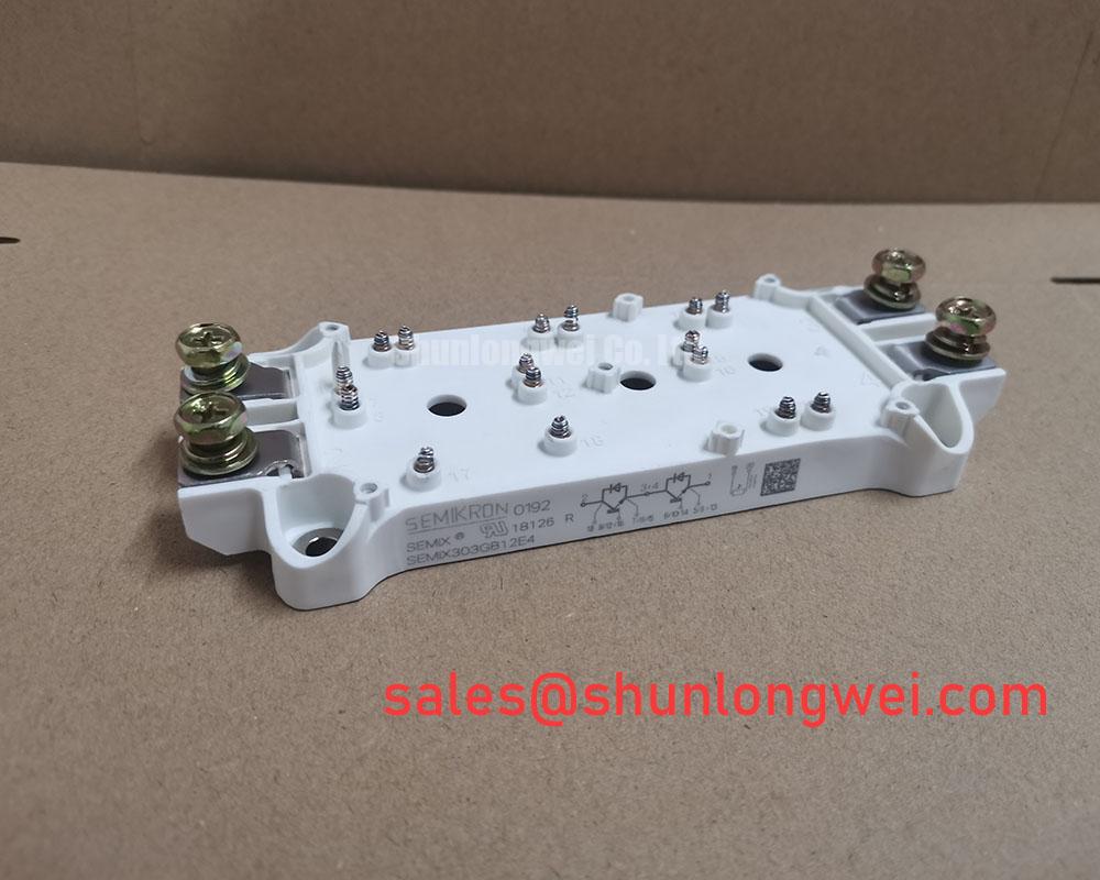
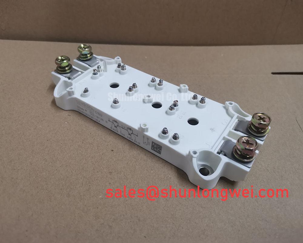
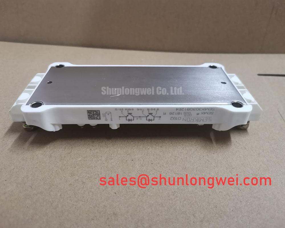
SEMIX303GB12E4-2 is a Semikron IGBT module in a SEMiX Module package. Its rated voltage is 1200 V, and its specified collector-current rating is 466 A under the stated conditions (Official Specifications).
Probe the gate-to-emitter and collector-to-emitter waveforms on each parallel switching position when a drive reports an intermittent overcurrent fault. Compare turn-on timing, turn-off timing and peak voltage under the same operating condition; a current imbalance seen only during switching calls for a different investigation from an imbalance that persists during conduction.
For SEMIX303GB12E4-2, the 1200 V and 466 A ratings establish device boundaries, not a guaranteed current share in a particular busbar assembly (Official Specifications). As a Design Consideration, closely matched power paths, gate-loop geometry and thermal interfaces can reduce differences between parallel positions. A positive temperature coefficient of collector-emitter saturation voltage can aid static sharing over an applicable operating region, but that behavior should not be assumed across all currents and temperatures without the relevant characteristic curves. Compare measured conduction voltage and case temperatures at matched loads before attributing an imbalance to the module.
Keep each gate-drive return close to its associated gate path, and separate sensitive drive wiring from high-current conductors where the terminal arrangement permits. Do not presume an auxiliary or Kelvin emitter connection without confirming the module’s terminal drawing. If one position turns on unexpectedly while its partner switches, inspect gate-to-emitter voltage for Miller-induced movement and assess the driver’s clamp arrangement against the installed circuit. Clearance and creepage at the terminals must be evaluated against the assembly’s working voltage, pollution environment and insulation design; the package name alone does not establish those distances.
For a comparison of electrical ratings and mechanical fit, SKM200GB12T4 is a reference for a separate compatibility review, not a presumed drop-in replacement. Confirm the circuit arrangement, terminal positions, driver requirements and cooling contact before making a substitution decision.
Benchtop Waveform Tuning: Mitigating Stress Through Mounting and Baseplate Contact on SEMIX303GB12E4-2
Check the module-to-heatsink contact pattern when switching waveforms deteriorate as the assembly warms. Uneven contact, trapped air or inconsistent mounting pressure can change the thermal conditions under which the waveforms were first recorded. Inspect both mating surfaces for damage and contamination, then follow the applicable mounting drawing for interface material, screw sequence and tightening torque. Do not transfer mounting instructions from a different SEMiX variant to this one.
A thin, continuous thermal interface is a Design Consideration: its purpose is to fill surface irregularities without introducing an unnecessarily thick insulating layer. Control application by the interface material’s instructions and inspect the resulting contact pattern rather than treating a proposed film thickness as an official SEMIX303GB12E4-2 specification. Account for baseplate shape through the approved mounting process; forcing a baseplate flat with uneven screw loading can compromise contact. Recheck mounting pressure after correcting a suspect interface, then repeat waveform measurements at a comparable temperature and load.
💡 Pro Tip: Keep the commutation paths geometrically balanced to limit turn-off overshoot, and verify the resulting voltage margin with controlled switching measurements. Record DC-link voltage and peak collector-emitter voltage at the module terminals so that busbar inductance is not mistaken for a change in device rating. If a fuse is part of the protection chain, evaluate its clearing behavior and let-through energy against the applicable device fault limits and the measured fault path; the 466 A current rating alone cannot establish fault-clearing coordination.
The surrounding power-stage schematic also matters. A module such as SKM50GB128D may appear in an equipment-level comparison, but its role and suitability must be determined from that equipment’s actual topology and ratings. Semikron Danfoss’s MiniSKiiP power-module information describes a different product line; family-level mounting or interface details should not be applied to this SEMiX module without matching documentation.
SEMIX303GB12E4-2 Circuit Protection & Reliability: Assessing Dynamic Power Loss and Multi-RC Thermal Models
Capture collector current, collector-emitter voltage and gate-to-emitter voltage during the overload pulse before changing protection settings. The traces show when current rises, whether the driver begins turn-off as intended and how high collector-emitter voltage climbs during interruption. Compare those observations with the protection circuit’s blanking, desaturation response and commanded dead time; do not infer a safe timing setting from the module’s current rating.
For pulsed loading, an Engineering Calculation can estimate junction-temperature rise by applying the time-varying device losses to an appropriate transient thermal-impedance model. Such a calculation requires the relevant loss characteristics, thermal model, initial temperature and cooling boundary conditions. None follows from the supplied 1200 V and 466 A ratings alone. If a multi-RC model is used, select coefficients documented for the device being assessed rather than borrowing them from another module, and compare calculated peak temperature with its specified junction limit.
Review turn-off and any diode commutation events separately. If the installed circuit uses an antiparallel freewheel path, reverse-recovery behavior can affect switching stress and radiated noise, but no recovery softness factor is established by the specifications stated here. Test the assembled circuit instead of assigning one. Likewise, evaluate Miller coupling and any active-clamp action from measured gate and collector waveforms under the actual bus voltage. The IGBT knowledge base provides background for interpreting these switching mechanisms; acceptance margins remain a system engineering decision.
Field Diagnostics & Commissioning: High-Altitude Voltage and Reliability Considerations in SEMIX303GB12E4-2 Topologies
Measure the maximum DC-link voltage and switching overshoot at the installed module when commissioning reveals voltage-related trips. Compare the observed peak with the 1200 V rated voltage (Official Specification), including operating states that can raise the link voltage. A 1500 V utility-scale solar inverter is only a potential equipment context: this 1200 V module must not be presumed suitable for a stage exposed directly to a 1500 V DC link. Assess the particular stage voltage and topology first.
For equipment installed at altitude, treat environmental effects on insulation coordination and voltage-headroom decisions as Design Considerations requiring an equipment-specific assessment. Terrestrial radiation can be relevant to high-voltage semiconductor reliability, but these product facts do not provide a device-specific single-event-burnout rate, failure-in-time figure or altitude derating curve. Do not calculate a service-life or failure-rate claim from altitude and nameplate voltage alone.
After a voltage-related trip, preserve fault records and compare the affected position with a known-good signal path: gate command, driver supply, gate-to-emitter response, collector-emitter peak and cooling condition. Investigate discrepancies without assigning a single cause to the trip. Commissioning limits should follow the verified module characteristics and the measured worst-case behavior of the completed power stage.