

Content last revised on November 4, 2026
Benchtop Waveform Tuning: Managing DC Bus Headroom on SEMIX453GB17E4IP
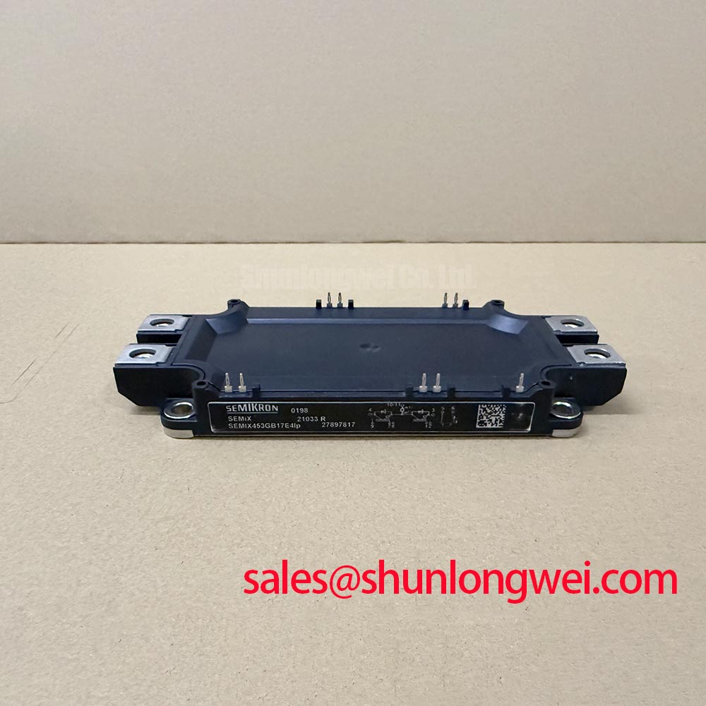
Before applying a replacement module to a high power inverter, isolate the DC link, inspect the power terminals and gate interface, then compare the cold state terminal behavior with a known good assembly. The SEMIX453GB17E4IP is specified for a collector emitter voltage of 1700 V at Tj = 25 °C and a continuous collector current of 450 A. Those are device ratings, not a complete operating prescription for a 1500 V central photovoltaic inverter. The switching frequency, DC link control, commutation path, cooling system, protection thresholds and transient environment remain system responsibilities.
When evaluating the module in a utility scale solar inverter, begin the waveform review at the actual DC link voltage used during startup, steady state operation and controlled shutdown. Compare the measured collector emitter waveform with the module rating while accounting for overshoot created by the commutation loop. A bus voltage that appears acceptable on a slow multimeter reading can still produce a damaging transient at turn off. Use a differential high voltage probe with a bandwidth suitable for the switching edge, and place the probe reference according to the test fixture safety procedure. The objective is to confirm the peak voltage and ringing behavior under the intended current and temperature conditions.
High altitude operation deserves a separate engineering review. Terrestrial neutron flux and other environmental effects can influence failure probability in high voltage power semiconductors, but a numerical Single Event Burnout rate or FIT value cannot be assigned to this module from the electrical ratings alone. A reliability assessment should combine the equipment altitude, shielding, mission profile, switching voltage distribution and a recognized reliability source. The practical field action is to record the operating altitude and DC link waveform, then establish a conservative operating envelope through controlled testing and documented system derating.
DC bus headroom derating should therefore be treated as a design consideration rather than a fixed percentage attached to the part number. Reduce the applied switching stress only after checking the required inverter output power, modulation range, peak current, thermal condition and protection response. At the bench, use a staged increase in DC link voltage while monitoring collector emitter overshoot, gate voltage, case temperature and current sharing. Stop the test when the waveform departs from the validated reference, even if the average bus voltage remains below the nominal system target.
Layout clearance also needs to be verified against the working voltage, pollution environment, enclosure geometry and applicable equipment standard. Keep high voltage copper away from gate control traces and measurement wiring, and avoid routing sensitive gate signals parallel to the collector switching path for long distances. The module itself does not provide an independent EMC approval for the complete inverter. The assembled system must be evaluated as a complete product, including the busbar, enclosure, cable harness, control board and protective earth arrangement.
For semiconductor platform context, engineers can consult the Semikron-Danfoss SEMITRANS® Industry Standard IGBTs reference and the Semikron-Danfoss Power Modules Catalog. These references help frame module families and application terminology, while the electrical limits for this product remain the values stated in its applicable product documentation.
SEMIX453GB17E4IP Operational Boundaries: DC Link Layout and Low Impedance Paths
The DC link capacitor bank should be positioned so that the high current commutation path is short, broad and mechanically stable. During a fast switching transition, stray inductance converts current slew into collector emitter voltage overshoot. In practical terms, the peak voltage rises with both the parasitic inductance and the rate of current change, so a compact laminated or carefully arranged bus structure is a design consideration for protecting voltage margin.
Inspect the capacitor connection, positive and negative bus geometry, module terminal contact and return path as one electrical loop. A capacitor with suitable nameplate capacitance can still perform poorly if its connection introduces excessive loop inductance or uneven current distribution. Check for loose hardware, discoloration, cracked insulation, lifted copper and asymmetric terminal pressure. A thermal image during a controlled load test can help locate abnormal resistance, but it should be interpreted together with current measurement and the switching waveform.
The stated VCE(sat) of 2.26 V typical applies at Ic = 450 A, VGE = 15 V and Tj = 150 °C. It is a defined test condition, not a universal value for every load current or junction temperature. When checking conduction behavior in the inverter, record collector current, gate voltage and temperature at the same time. A rising saturation voltage may reflect temperature, gate drive quality, current imbalance, connection resistance or a developing semiconductor fault. Use the complete set of measurements instead of assigning a single cause from one voltage reading.
Short circuit protection must be coordinated with the gate driver and the power stage. Desaturation detection, blanking behavior and soft turn off are system functions that require timing validation against the actual driver, isolation barrier and module switching loop. The module ratings supplied here do not establish a universal short circuit withstand time or a mandatory detection interval. During commissioning, verify that the protection circuit detects an abnormal collector emitter condition before the energy in the DC link and commutation loop exceeds the validated test boundary.
A two stage soft turn off strategy can be considered where the inverter architecture requires reduced voltage overshoot during a fault. The first stage limits gate drive energy, and the second stage completes turn off with controlled current change. The appropriate thresholds, delay and gate resistance depend on the driver, bus inductance, fault current and measured waveform. They should be tuned on the actual power assembly rather than copied from an unrelated module family.
Field Alert: Never connect or remove the gate harness while the DC link or auxiliary gate supply is energized; follow the equipment isolation and discharge procedure before service.
For a cross reference review, the SKET400/08E is a separate product that may be evaluated as part of a broader power semiconductor comparison. Its electrical ratings, topology and mechanical interface must be checked independently before any substitution decision. The SEMIX453GB17E4IP should be treated as a direct candidate only where the original inverter documentation confirms electrical, mechanical, thermal and gate drive compatibility.
SEMIX453GB17E4IP Thermal Electrical Optimization: Turn Off and Recovery Stress
Turn off behavior should be reviewed alongside the antiparallel diode recovery waveform. Reverse recovery current can add to the active switching current and increase voltage stress in the commutation loop. A sharp recovery transition may also excite ringing in the busbar, capacitor connection and gate loop. On the bench, capture collector current, collector emitter voltage and gate emitter voltage on the same time base while repeating the test at relevant current and temperature points.
The module provides an official total power dissipation of 2500 W per IGBT at Tc = 25 °C and a specified junction to case thermal resistance of 0.06 K/W per IGBT. These values describe defined thermal conditions and should not be converted directly into a guaranteed field operating temperature without the complete heatsink, interface material, mounting structure, airflow and power waveform. The official operating junction temperature range is −40 °C to +175 °C.
For pulsed inverter operation, the instantaneous junction temperature depends on the thermal impedance response to the load pulse, not only on average power. An engineering calculation may use the module thermal impedance network together with the measured switching and conduction losses, but the resulting temperature estimate is only as reliable as the loss model and thermal interface measurements. Validate the estimate with case temperature, coolant or heatsink data and the actual duty cycle.
Gate loop damping is another practical tuning point. Minimize the physical loop area between the gate driver output, gate terminal and emitter return, and keep the power switching current out of the gate return path. A separate gate return route can reduce unwanted feedback, but the final routing must respect the actual module terminal arrangement and driver reference. Adjust turn on gate resistance only after observing gate voltage overshoot, plateau behavior and collector current transition on the assembled inverter.
Snubber selection follows the measured transient rather than a generic capacitor value. An RC network can reduce ringing when its impedance and placement match the dominant parasitic loop, but excessive capacitance increases switching loss and may alter thermal loading. Start from the measured ringing frequency and energy, then compare the effect of candidate networks during double pulse or equivalent controlled switching tests. The result must be checked against the Vces rating of 1700 V and the system DC link operating envelope.
Long motor or transformer cables can behave as transmission paths. Reflections at the far end may return toward the inverter and combine with local switching overshoot. This is relevant when a central inverter feeds a remote transformer or long AC connection. Cable impedance, termination, transformer leakage characteristics and switching edge rate determine the observed waveform. Review the complete power path rather than treating a cable filter as an automatic remedy.
SEMIX453GB17E4IP Circuit Protection and Isolation Integrity
Gate drive isolation must be verified as part of the complete control assembly because the IGBT module ratings do not by themselves specify the reinforced insulation performance, common mode transient immunity or certification status of an external optocoupler or digital isolator. Check the gate driver datasheet, isolation test documentation, creepage and clearance layout, insulation system and power supply arrangement together.
Common mode voltage changes at the switching node can couple into the isolated gate command through parasitic capacitance, probe wiring, heatsink structure and auxiliary supply paths. A false gate pulse may appear as abnormal gate movement, unexpected current overlap or irregular turn off timing. Verify the gate signal at the module terminals with an appropriately rated isolated measurement setup, then compare it with the driver input signal. The time relationship between the two signals is more useful than a visual inspection of the controller waveform alone.
Keep the isolated control return physically separated from the high current emitter path unless the module and driver architecture explicitly requires a shared reference. Where an auxiliary emitter connection is provided by the specific assembly, route it according to the applicable terminal drawing and use it consistently for the gate measurement reference. Do not assume that a visually convenient copper connection provides the same switching behavior as the intended control return.
The VGE(th) value of 5.8 V typical at Ic = 18 mA is a threshold test condition, not a recommended gate drive voltage. A system integrator should verify the positive gate supply, turn off bias, gate resistance, clamp behavior and driver current capability from the original inverter design and the applicable module documentation. Gate voltage must remain within the approved operating boundary during normal switching, fault turn off and power sequencing.
Protection coordination should include DC link discharge, gate supply undervoltage handling, driver fault latching and restart sequencing. A module that measures correctly at room temperature can still be exposed to excessive electrical stress if the driver restarts while the DC link is not in the expected state. Use a controlled fault injection procedure to verify that the gate outputs remain inactive during an isolation fault, auxiliary supply collapse or desaturation event.
For system level technical context on high voltage switching structures and alternative semiconductor approaches, see The 1200 V CoolSiC™ MOSFET Advantage in Three. That discussion concerns a different semiconductor technology and voltage class; it should inform topology comparison only, not be treated as a substitute specification for the Semikron SEMIX453GB17E4IP.
When this module is evaluated for a utility scale 1500 V central photovoltaic inverter, the final release decision should join the electrical rating review with the measured switching waveform, thermal impedance assessment, isolation verification, protection timing and mechanical installation inspection. The documented product values remain 1700 V Vces, 450 A continuous collector current, 2.26 V typical VCE(sat) under the stated test condition, 2500 W per IGBT at Tc = 25 °C, 0.06 K/W junction to case thermal resistance and an operating junction range of −40 °C to +175 °C.