Content last revised on November 4, 2026
SEMIX604GB176HDS Semikron 1700V 400A IGBT Module
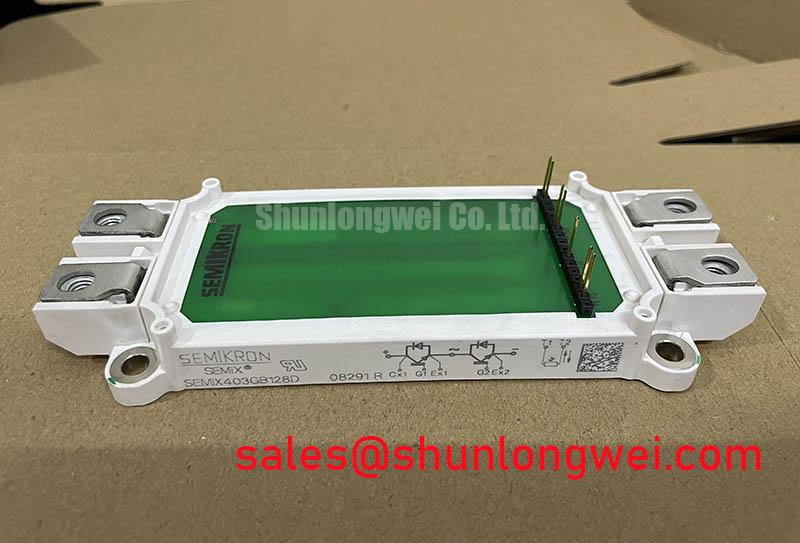
With power isolated and the DC link discharged according to the equipment procedure, measure the disconnected power terminals for unintended low resistance, inspect the SEMiX housing for cracks or distortion, and compare the nameplate with the replacement record before reconnecting the DC link. The SEMIX604GB176HDS is a Semikron IGBT Module specified at 1700.0 V and 400.0 A, with a SEMiX Module housing. These identity values should be checked against the original manufacturer documentation when checking a failed converter position or preparing a controlled replacement assessment.
For a multi megawatt offshore or onshore wind turbine full scale converter, these ratings identify the electrical class of the device, but they do not by themselves establish the allowable DC link voltage, switching frequency, overload duration, thermal cycle, or protection threshold in the installed cabinet. The service engineer must match the module to the original gate driver, busbar geometry, cooling assembly, fuse coordination, and control firmware.
The Semikron Danfoss Power Electronics and Modules Official Hub provides the appropriate manufacturer level reference environment for power module families. Product line names and package conventions should not be assumed to define the internal terminal arrangement of this specific part.
Assembly Integrity and Layout Architecture: Assessing Cosmic Ray Risk for SEMIX604GB176HDS
At elevated installation sites, review the DC link operating point together with switching transients rather than treating the 1700.0 V rating as a complete system voltage limit. Terrestrial neutron exposure can contribute to single event burnout risk in high voltage power semiconductors, but a defensible FIT or SEB calculation requires a qualified device failure model, mission profile, altitude spectrum, voltage waveform, junction temperature history, and an authoritative source.
The practical field task is to capture the highest device voltage during turn off and abnormal commutation, then compare that measured stress with the approved design limit for the selected module and system. Use a properly rated differential probe and a measurement arrangement that does not add excessive loop inductance. Check the voltage at the module terminals, not only at a remote DC link capacitor, because busbar inductance can create a local overshoot that is invisible at the capacitor.
Layout work should keep the commutation path compact, symmetrical, and mechanically supported. Minimize parasitic inductance in the high current loop to suppress turn off overshoot, and route gate drive and emitter return conductors so that power current does not share the driver reference path. Clearance and creepage must be selected from the actual working voltage, pollution environment, insulation system, altitude, and applicable equipment standard. The system designer remains responsible for verifying the resulting margins during switching tests.
When investigating a repeated high voltage failure, record the DC link waveform, gate voltage at the module pins, cooling condition, fault timestamp, and switching state. A single damaged module does not establish cosmic ray involvement; the same symptom may also follow excessive commutation inductance, gate control malfunction, overtemperature, or an incorrectly coordinated protection circuit. For broader application context on converter stress evaluation, consult the Industrial Applications reference.
Assembly Integrity and Layout Architecture: Terminal Screw Engagement and Fuse Coordination
Mechanical installation begins with the original terminal drawing and the hardware specified for the power interface. Confirm that the screw length, washer stack, thread engagement, conductor lug, and busbar thickness do not allow the fastener to bottom out or transfer levering force into the module terminal. The busbar should lie naturally against the terminal surface; pulling it into position with the screw can stress internal copper joints and create a fault that appears only after vibration or thermal cycling.
Field Alert: Apply the terminal tightening method and torque specified for the actual fastener and module assembly, and use a uniform, thin thermal interface layer where the cooling design requires it.
After installation, inspect the busbar for tilt, witness marks, and uneven washer compression. Check that the power conductors are independently supported so cable weight and cabinet vibration are not carried by the semiconductor terminal. Repeat the mechanical inspection after the initial thermal run if the equipment maintenance procedure requires it.
| Parameter | SEMIX604GB176HDS | Replacement assessment reference |
|---|---|---|
| Manufacturer | Semikron | Confirm the original bill of materials and service documentation |
| Product category | IGBT Module | Use the same functional topology and terminal arrangement |
| Rated voltage | 1700.0 V | Compare the installed DC link and measured switching peak |
| Rated current | 400.0 A | Confirm the manufacturer's rating conditions and compare load profile, cooling, pulse duration, and protection settings |
| Housing | SEMiX Module | Verify mounting footprint, terminal positions, and cooling interface |
High speed fuse coordination is a system calculation. The fuse clearing characteristic, available fault current, wiring inductance, gate turn off behavior, and the module short circuit or surge capability must be evaluated together. Do not select a fuse solely from the 400.0 A label. Where applicable withstand data are available for the fault path, compare them with the fuse clearing integral under the relevant operating conditions. A fuse clearing integral alone does not establish IGBT short circuit protection. Protection coordination also needs to account for detection delay and the time required for the gate driver to reduce current.
For broader material planning, engineers may review the SKET400/08E as a separate Semikron thyristor device reference. It is not a replacement for this IGBT module. Any proposed IGBT replacement requires checks of pin arrangement, electrical topology, voltage class, thermal interface, gate requirements, and mechanical dimensions before a substitution decision.
Field Diagnostics and Commissioning: Separating Driver Return from Main Current
Gate driver return routing must be checked against the physical terminal definition before commissioning. A main emitter connection carries load current, while an auxiliary or Kelvin emitter connection, where provided by the specific module arrangement, is intended to give the driver a cleaner reference. The two paths must not be joined casually at a distant busbar or through a conductor that also carries commutation current.
Start with the module drawing and cabinet wiring record. Identify collector, emitter, gate, and any auxiliary emitter or sensing terminals by their documented designations. With power isolated and the DC link discharged according to the equipment procedure, trace each driver return conductor to its driver board. Look for shared copper, loose crimp joints, parallel high current conductors, and connectors whose pin numbering changes between the module and the driver harness.
During a controlled low energy test, observe the gate to its intended emitter reference directly at the module terminals. A waveform that looks acceptable at the driver board can differ at the module because of common emitter inductance and ground bounce. False turn on, uneven parallel device behavior, excessive ringing, or an apparent dead time change should lead to a complete gate loop inspection rather than an immediate module replacement.
Where multiple IGBTs operate in parallel, positive temperature coefficient behavior can support static current sharing, but it does not remove the need to match layout impedance, gate loop characteristics, switching timing, and thermal coupling. Dynamic sharing is determined during the transition, so the system engineer should compare gate waveforms and collector emitter voltage behavior for each device position. Dead time must prevent cross conduction under the actual driver delay, propagation variation, and switching conditions. Any buffer or soft turn off function should be validated against the installed desaturation or overcurrent protection scheme.
The Semikron MiniSKiiP power module reference is useful for understanding manufacturer terminology across module families, but it does not replace the terminal and gate documentation for the SEMiX assembly under service.
SEMIX604GB176HDS Operational Boundaries: Thermal Capacitance and Heat Sink Limits
Thermal acceptance during pulsed overload depends on the complete transient path from semiconductor junction to case, interface, heat sink, coolant, and enclosure. A short current pulse may be tolerated differently from continuous operation because thermal capacitance delays case temperature rise while the junction temperature can still move rapidly. Use the approved transient thermal impedance data for the device and combine it with the measured pulse profile rather than converting the 400.0 A rating into a universal overload command.
For commissioning, log phase current, pulse duration, repetition pattern, case temperature, coolant or heat sink condition, and the point at which protection operates. The thermal model should represent the actual load sequence, including repeated acceleration, regeneration, grid disturbance, and recovery intervals where applicable. A multi section resistance capacitance model can then estimate junction temperature from power loss over time, provided its parameters come from an authoritative device or assembly source.
Inspect the cooling interface when the measured thermal response differs between otherwise comparable phases. Uneven compound coverage, a warped mounting surface, loose fasteners, blocked coolant channels, or a displaced temperature sensor can all distort the result. Mechanical flatness and interface preparation should follow the module and heat sink instructions; the service record should retain the measured temperatures and operating conditions.
During a fault event, do not rely on a single thermal sensor to determine whether the module is healthy. Compare phase current balance, gate command timing, voltage overshoot, case temperature trend, and protection logs. If a module is replaced, preserve the original busbar alignment and driver harness arrangement, then repeat the controlled commissioning checks with the converter disabled from full energy operation until the electrical and thermal behavior is consistent.