
Content last revised on October 14, 2026
Assembly Integrity and Layout Architecture: Gate Drive Resistance Calibration for SKIIP32NAC12T42
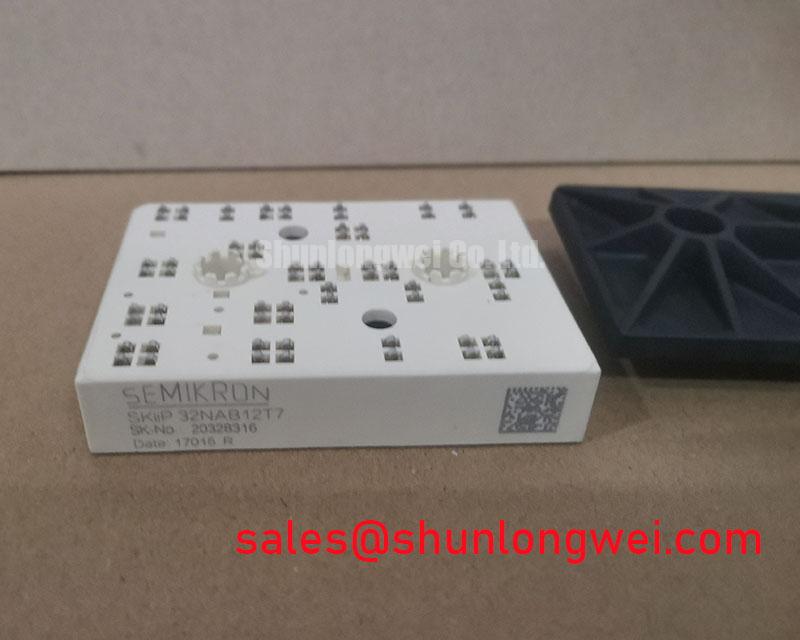
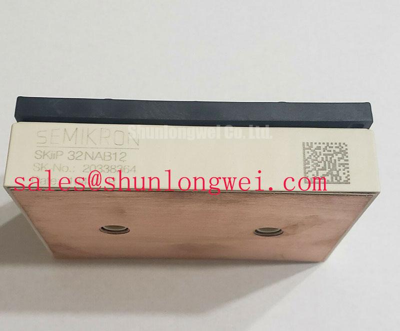
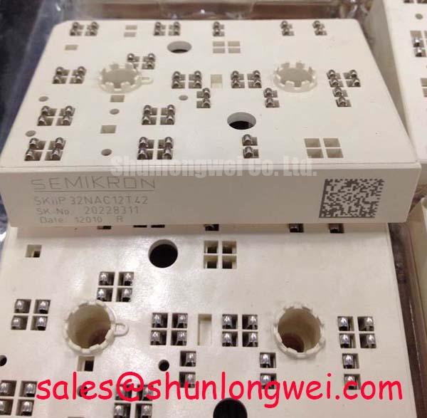
When a legacy inverter board is fitted with SKIIP32NAC12T42, start at the gate driver interface rather than changing protection thresholds immediately. Confirm the gate return path, inspect the driver supply under switching load, and compare the existing gate resistor network with the switching behavior of the replacement module. The device is specified as a 1200 V, 32 A Semikron IPM in a MiniSKiiP / SKiiP package, but the surrounding driver, busbar, load cable, and control timing determine whether that electrical rating can be used without excessive switching stress.
External turn-on and turn-off resistance should be treated as separate tuning elements when the circuit allows it. A lower turn-on resistance can increase gate current and reduce switching transition time, but it can also increase collector current slew rate, diode recovery interaction, and radiated noise. A higher turn-on resistance generally slows the transition and may reduce ringing, at the cost of increased switching loss. Turn-off resistance has a different role because it controls how quickly stored gate charge is removed while the power loop is developing its highest voltage excursion.
For a retrofit, record the original resistor values, gate trace length, driver output arrangement, and emitter reference before making changes. A legacy PCB may have been tuned around a different internal gate charge, diode recovery profile, or power loop geometry. Reusing the original resistor value without checking the gate waveform can create a mismatch even when the module fits mechanically. The practical measurement is the gate to emitter voltage at the module terminals, not the voltage observed at the driver IC pins. Probe placement should use the shortest practical loop, because a long probe ground connection can introduce ringing that does not exist in the module gate circuit.
Gate resistance calibration should be performed while monitoring the collector emitter voltage, phase current, and driver supply. During turn-on, look for the interaction between the IGBT transition and the antiparallel diode recovery current in the opposing device. During turn-off, compare the voltage overshoot with the DC link operating condition and confirm that the gate signal remains controlled during the Miller interval. The correct setting is a system result: it must balance switching loss, peak voltage, current slew rate, audible behavior, and electromagnetic compatibility in the actual inverter assembly.
Gate loop geometry is as important as resistor selection. Keep the outgoing gate path and gate return path close together, avoid routing them beside high current commutation conductors, and maintain a clean reference connection back to the driver. Common mode ground bounce can appear as an unwanted gate pulse or as an apparent negative excursion at the emitter reference. If the driver provides a negative turn-off bias, the value and timing remain system-dependent; verify the driver’s common-mode capability and the module’s permitted gate-emitter operating range before applying it.
When evaluating a compact industrial inverter or high-speed CNC spindle drive, check the complete commutation loop from DC link capacitor to module terminals and back to the capacitor. A symmetrical laminated busbar arrangement can reduce parasitic inductance, but the final result must be measured at the module terminals during switching. The same review applies when comparing a related unit such as SKIIP 13NAB12T4V1; package compatibility alone does not establish electrical interchangeability.
💡 Pro Tip: Keep the power and gate return paths physically compact and confirm the turn-off voltage margin with a properly connected differential probe before increasing switching speed.
Transient Dynamics and Electrical Design: Antiparallel Freewheeling Diode Reverse Recovery in SKIIP32NAC12T42
Reverse recovery evaluation should begin at the commutation event where the antiparallel diode changes from forward conduction to reverse blocking. The measured peak recovery current, reverse recovery time, and recovery softness influence the voltage overshoot seen by the opposite IGBT. These values should be taken from the applicable device documentation or switching test data for the exact configuration rather than inferred from the module’s 1200 V voltage class or 32 A current rating.
A hard or “snappy” recovery event can create a steep current change through the stray inductance of the commutation loop. That interaction may produce local voltage ringing, increased common mode current, and electromagnetic radiation around the inverter cabinet. The first corrective action is usually to review the physical current path and gate drive timing. A snubber fitted across the wrong physical nodes may have limited effect, while a correctly located network can reduce the high frequency component seen by the switching loop.
RC snubber selection is an engineering recommendation based on measured ringing frequency, peak voltage, pulse energy, repetition rate, and capacitor dielectric behavior. The resistor must tolerate repetitive pulse energy, and the capacitor must have suitable voltage, dv/dt, and temperature characteristics for the switching environment. Do not treat an RC network as a substitute for poor busbar geometry. The snubber connection should be short, wide, and placed across the relevant switching nodes so that its current does not travel through an unnecessarily large loop.
Turn-on gate resistance can be adjusted to manage the interaction between the incoming IGBT and the recovering diode. Increasing the resistance may reduce the current edge rate and soften the commutation event, though it can increase turn-on loss and thermal loading. Reducing the resistance may improve switching efficiency while increasing overshoot and electromagnetic stress. Use a controlled test sequence and compare the module terminal waveform, phase current, heatsink temperature, and driver behavior after each change.
Phase-angle conduction and line-frequency ripple smoothing also affect the conditions under which the diode operates. In a front-end or regenerative topology, the DC link capacitor, rectifier stage, load power factor, and control angle determine the current waveform presented to the inverter bridge. A related module such as SKIIP12AC126V1 may appear in the upstream rectification or complementary power path, but its presence does not define the switching behavior of this IPM. Each stage should be evaluated according to its own conduction interval, thermal path, and transient current.
For a high-speed CNC spindle drive, the motor cable adds another variable. A long cable can behave as a transmission path, producing reflected voltage at the motor terminals and additional stress at the inverter output. Cable construction, motor impedance, termination, carrier frequency, and output filter selection determine the magnitude and timing of the reflected wave. The suitable mitigation may involve output filtering, controlled edge rates, or a revised cable arrangement; the system designer should verify the motor-side waveform rather than assigning the entire event to the power module.
During troubleshooting, use a differential high-voltage probe at the module switching node and a current probe around the intended commutation conductor. Compare the waveforms with the snubber disconnected and connected only when the test arrangement is safe and repeatable. Look for changes in peak voltage, ringing duration, current recovery shape, and driver disturbance. If an RC network reduces ringing but raises average temperature, its pulse loss must be included in the thermal assessment. If it has little visible influence, inspect its physical connection and measurement bandwidth before changing component values.
The Semikron references for MiniSKiiP power modules and SKiiP technology provide useful background for understanding the product family and its mechanical integration approach. System-level compliance remains dependent on the complete inverter, enclosure, cabling, grounding, and filter arrangement; an individual IPM does not independently establish EMC compliance for the finished equipment.
Assembly Integrity and Layout Architecture: Terminal Screw Engagement Depth for SKIIP32NAC12T42
Terminal installation should preserve both electrical contact quality and the mechanical neutrality of the module base and internal current paths. Before fitting the busbar, confirm that the screw length, washer stack, terminal opening, and mating conductor thickness match the module’s mechanical drawing. Excessive engagement can bottom out inside the terminal or apply force to internal conductive parts, while insufficient engagement can reduce contact stability during vibration and thermal cycling.
Use a flat, clean mating surface and keep the busbar aligned with the terminal before tightening. A misaligned conductor can introduce a sideways load that is transferred into the module terminal and its internal copper joins. This is particularly important in compact inverter assemblies where a rigid laminated busbar may pull against the module as the enclosure or heatsink expands. The busbar should be supported independently where necessary so that the terminal fastener provides electrical clamping rather than correcting a mechanical alignment error.
Washer selection influences how the clamping load is distributed. A suitable washer should support the conductor without damaging the terminal surface, and the tightening sequence should follow the equipment assembly procedure. Apply the specified torque from the applicable mechanical documentation using a calibrated tool; do not substitute a generic torque value when the module or busbar manufacturer provides a different requirement. Recheck that the conductor has not shifted after tightening, especially where several phase terminals are assembled in a confined space.
Clearance and creepage must be reviewed around the complete terminal arrangement, not only across the visible package surface. Maintain the required separation between the DC link, phase output, control terminals, heatsink structures, and grounded chassis according to the equipment insulation design and applicable standard. Remove conductive debris, loose strands, and excess hardware from the power compartment. The 1200 V class of SKIIP32NAC12T42 makes the physical arrangement of high-voltage conductors a design matter, while the final insulation coordination belongs to the finished equipment.
After assembly, inspect the terminal interface for tilted washers, uneven conductor contact, damaged plating, and interference with nearby molded features. Check continuity through the intended power path with the equipment isolated, then verify that no control terminal has been shorted to a power terminal or heatsink. A cold resistance reading can identify an open connection or an unexpected short, but it cannot prove that the joint will remain stable under switching current, vibration, or thermal cycling.
Thermal interface preparation should also be handled consistently across the mounting surface. The heatsink, module base, and interface material must be clean and free from particles that could create local pressure points. Mounting the module while the busbar is forcing it into position can distort the assembly and compromise thermal contact. Complete the mechanical mounting sequence first, then align the electrical conductors without using the terminal screws as structural levers.
For field replacement in a compact industrial inverter, document the original conductor orientation, terminal labeling, gate connector position, and heatsink arrangement before removal. Photographing the busbar path can prevent phase order errors during reassembly. After power wiring is complete, conduct a low-energy control check before applying full DC link voltage. Confirm gate timing, interlock behavior, and current feedback operation while watching for unexpected driver supply movement or simultaneous conduction commands.
Reliability-focused design should also consider the relationship between mechanical assembly and electrical transients. A loose or uneven terminal joint can add localized heating, while excessive mechanical stress can change contact behavior during temperature cycling. The engineering reference The Ultimate IGBT Knowledge Base can support broader review of switching behavior, thermal paths, and failure mechanisms when the module is being integrated into a revised power stage.
When the module is evaluated as a replacement in a CNC spindle drive, verify phase sequence, motor rotation, current scaling, braking behavior, and output waveform under controlled operating conditions. The product category and package provide a starting point for mechanical and electrical assessment, but the final acceptance test belongs to the assembled inverter and its connected motor system.