Content last revised on October 30, 2026
SKIIP32NAB12T10 Thermal-Electrical Optimization: Fault-Clearing Dynamics and Type-I/II Desaturation Tuning
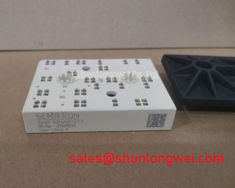
Isolate the drive supply, verify that the DC link has discharged, and compare cold-state readings between equivalent power terminals before reconnecting the gate-driver board. On the Semikron SKIIP32NAB12T10, separate the inverter, rectifier, and brake-chopper paths on the circuit diagram before interpreting a low-resistance reading; parallel circuitry can otherwise obscure which section needs further investigation.
The official specifications distinguish an inverter collector-emitter blocking voltage of 1200 V, a rectifier repetitive peak reverse voltage of 1600 V, and a brake-chopper collector current of 20 A at 80°C case temperature. An integrated NTC thermistor provides temperature-dependent resistance for the equipment’s monitoring circuit. These ratings belong to different functions: the brake-chopper current is not an inverter output-current rating, and the rectifier voltage rating must not be assigned to the IGBT section.
Capture the gate command, gate-emitter voltage, collector-emitter voltage, and driver fault response on a common time reference when investigating a desaturation trip. As a Design Consideration, the useful measurement is the complete interval between fault development and current interruption, not simply the delay between a controller command and a fault indication. Probe isolation, voltage capability, and connection geometry must suit the measurement location without introducing an unintended earth connection.
A Type-I short circuit describes turn-on into an existing short circuit; a Type-II event develops while the device is already conducting. The distinction matters because the current rise, collector voltage trajectory, and gate behavior differ. Desaturation blanking must accommodate normal switching without concealing a developing fault. Its setting therefore belongs to the coordinated driver and power-stage design, evaluated against the device’s documented short-circuit safe operating area rather than an assumed universal microsecond limit.
For an existing machine, inspect the desaturation sensing path before changing its threshold or timing. Contamination, damaged sensing components, altered return routing, and a weak driver supply can affect the observed response. Compare the suspect channel with an equivalent healthy channel under controlled conditions. A desaturation alarm alone does not distinguish an actual load short circuit from a sensing-path disturbance or incomplete IGBT enhancement.
Two-stage soft turn-off is a Design Consideration when the external driver supports it. A controlled initial gate discharge can reduce the abrupt current change that produces inductive overshoot, followed by a firm off state. Excessively slow interruption also increases fault energy, so the waveform must demonstrate acceptable collector-voltage stress and timely current extinction together. Active clamping requires the same coordination; it is not a substitute for correcting excessive commutation-loop inductance.
Check complementary gate signals at the power-device connections rather than relying only on controller-side timing. Propagation-delay differences, gate discharge behavior, and temperature affect the effective dead time. Too little separation can permit cross-conduction; unnecessarily long separation increases diode conduction and can alter current distortion. Establish the timing from measured switching behavior across the equipment’s intended operating conditions, without treating a generic dead-time setting as a SKIIP32NAB12T10 specification.
Miller-induced gate movement deserves attention when a fault appears only during fast switching. Reverse-transfer capacitance couples collector-voltage changes into the gate circuit, whereas Miller plateau charge describes charge transferred during that switching interval; the two are related but not interchangeable quantities. Evaluate the gate return path, driver sink capability, and any supported Miller clamp against the measured off-state gate excursion. Avoid inferring clamp requirements from the blocking-voltage rating alone.
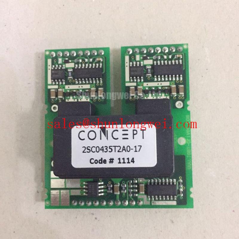
If the external driver uses a bootstrap supply, examine its voltage during the actual modulation sequence, including operating points with limited recharge opportunities. Capacitor charging, diode behavior, driver consumption, and switching-node transients can affect the available gate supply. Likewise, assess the optocoupler or digital isolator’s common-mode transient immunity against the measured disturbance at its isolation barrier. The Semikron MiniSKiiP® Power Modules resource provides manufacturer product-family context; driver capabilities must still be established from the installed driver hardware.
Field Diagnostics & Commissioning: Mounting Contact and Screw Tightening for SKIIP32NAB12T10
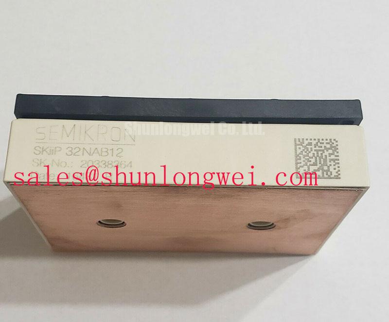
Inspect the heatsink contact surface and mounting stack before tightening the replacement assembly. As an Engineering Recommendation, remove old interface residue using a compatible cleaning method, check for burrs and contamination, and examine the previous contact pattern for uneven pressure. Do not assume that a generic metal-baseplate mounting method applies to this module’s construction; the contact arrangement and fastening procedure must follow the applicable module assembly instructions.
Thermal interface material should fill surface irregularities without becoming an unnecessarily thick thermal barrier. Apply the material and coverage pattern specified for the assembly, then inspect for displacement or incomplete coverage during an approved fit check. A generic thickness recommendation cannot establish the correct bond line for this part. Likewise, apparent curvature should prompt a check of the mounting surfaces and specified tolerances, not improvised flattening, shimming, or increased screw force.
Field Alert: Follow the module-specific tightening sequence and torque requirements, and never use extra screw force to compensate for an uneven heatsink or excessive thermal interface material.
Where the assembly instructions require progressive tightening, bring the mounting points into engagement in that sequence rather than fully loading one location first. Check that the surrounding circuit board, connectors, and mechanical supports are not imposing additional strain. A replacement that fits the mounting holes can still have an incompatible contact arrangement or terminal geometry, so mechanical acceptance should include the complete installed stack.
The integrated NTC thermistor should be checked through its actual monitoring circuit. Compare its resistance response as temperature changes and inspect the harness and input circuitry for intermittent behavior. The controller’s conversion curve must match the sensor characteristic. Treat the reported temperature as a measurement at the sensor location, not as a direct, instantaneous measurement of every semiconductor junction during a switching event.
Keep rectifier troubleshooting separate from inverter switching analysis. A diode rectifier does not acquire phase-angle control merely because the surrounding drive uses controlled switching. Trace the input bridge, precharge circuit, DC-link components, and brake-chopper branch individually. Line-frequency ripple depends on the supply and loading conditions as well as the DC-link network; inspecting ripple can help locate a problem, but it does not by itself identify a failed module.
For topology comparisons, the manufacturer’s Semikron SEMIPACK® Thyristor / Diode Modules resource distinguishes rectifying and controlled-rectifying component families. If an equipment schematic includes a separate auxiliary switching stage, a part such as SKM150GAL12T4 should be evaluated by its own circuit function and documentation, not treated as an interchangeable front-end rectifier.
When an RC snubber is present, inspect its connections and component condition before changing values. Its damping effect depends on the parasitic network and switching behavior at that location. A snubber can suppress a measured oscillation, but it cannot correct a poor mechanical thermal contact. Keep those investigations separate so that reduced ringing is not mistaken for restored thermal performance.
Benchtop Waveform Tuning: Mitigating Stress via Output Sinusoidal Filter vs dv/dt Reactor on SKIIP32NAB12T10
Compare the waveform at the inverter output with the waveform at the motor terminals when investigating cable-related voltage stress. As a Design Consideration, an impedance mismatch between the drive, cable, and motor can produce reflected-wave overshoot. Its magnitude depends on the transition time, cable characteristics, termination, and pulse sequence; a fixed voltage multiplier is not a guaranteed behavior of the SKIIP32NAB12T10.
Use a consistent probing method at both locations and record the operating condition with each capture. A voltage peak measured at the motor does not automatically equal the collector-emitter stress inside the inverter. Conversely, local switching-loop overshoot can stress the semiconductor without producing an identical motor-terminal waveform. Separating these measurement locations prevents an output-filter change from being used to address the wrong transient.
A dv/dt filter primarily moderates voltage transitions reaching the cable and motor, while a sinusoidal output filter more extensively attenuates switching-frequency content. Selection should account for the drive’s switching strategy, output frequency range, motor current, cable arrangement, and filter manufacturer’s operating restrictions. Filter inductance, capacitance, damping, and thermal capacity are system-level choices; the module’s blocking-voltage rating does not determine them.
Before approving either approach, examine how the added network affects current regulation and protection. Filter voltage drop can alter the available motor voltage, and resonance can affect current waveforms or control stability. Check the drive manufacturer’s permitted filter arrangements and assess startup, low-speed operation, load transitions, and deceleration. Keep power and sensing routes arranged to limit unwanted coupling, with clearances established from the equipment’s applicable insulation requirements.
Freewheeling-diode recovery also influences switching stress. During commutation, recovery current interacts with loop inductance and device switching speed, affecting ringing and conducted disturbance. Recovery softness describes the shape of that recovery process; it is not an independently established value for this model here. Compare current and voltage captures under matched conditions before attributing a change in interference to the diode alone, and assess electromagnetic compatibility at equipment level rather than assigning it to the module.
For light industrial automation or multi-joint robotic articulator drives, compatibility evaluation should include regeneration, repeated acceleration, and the installed motor-cable arrangement. Compare the SKIIP82AC121T1 only as a separate reference candidate: matching a voltage class does not establish equivalent topology, pin assignment, thermal behavior, or protection requirements. Record those differences explicitly before considering any substitution.
The technical article The 1200 V CoolSiC™ MOSFET Advantage in Three-Phase Power Conversion offers complementary context for technology comparisons, not evidence of this IGBT module’s lifetime or switching limits. For the repaired assembly, retain the verified gate timing, fault-response captures, thermal contact observations, and inverter-to-motor waveform comparison. If an output filter is changed, repeat the affected control and protection checks before returning the equipment to its approved operating sequence.