

Content last revised on October 13, 2026
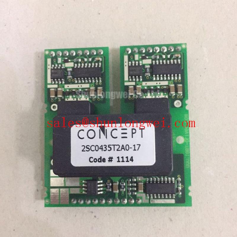
Field Diagnostics & Commissioning: Preventing High di/dt Gate Loop-Induced Transients in 2SC0435T2A0-17 Topologies
Separate the load emitter path from the gate-reference return wherever the connected IGBT module provides a documented auxiliary emitter terminal. This is a Design Consideration for the external power stage, not a claim that the driver board itself contains a Kelvin emitter terminal. The auxiliary return should reference the gate driver to the switching device without sharing the voltage drop produced by load-current commutation.
Follow the gate conductor and its return as a complete loop. Connector transitions, long adapter tracks, and shared return copper can undermine an otherwise compact assembly. Keep the outgoing and returning paths close together while preserving the separation required between control circuitry and power conductors. Clearance and creepage depend on the complete assembly’s working voltage, insulation requirements, contamination conditions, and construction; board fit alone does not establish electrical suitability.
For waveform diagnosis, measure gate-to-emitter voltage at the power module terminals using a suitably rated differential measurement arrangement. Compare that waveform with the driver-side output during the same switching event. A difference can indicate interconnect inductance or reference movement, but probe pickup must also be excluded. Examine unintended gate excursions alongside collector voltage and load current rather than interpreting a single ringing trace as proof of false turn-on.
Miller coupling provides another route for an inactive IGBT’s gate voltage to rise during commutation. As a Design Consideration, evaluate the complete off-state discharge path, including gate resistance, connector impedance, and driver behavior. The discussion in Evolution of Negative Off-Bias Gate Drive Circuits provides background for assessing off-state bias strategies; it does not establish a particular bias setting for this board.
When evaluating the driver for light industrial automation or multi-joint robotic actuator drives, compare the controller interface, fault-response path, and semiconductor gate requirements with the existing assembly. A higher peak output-current capability does not independently establish compatibility with the original switching speed or protection coordination.
Assembly Integrity & Layout Architecture: Implementing and Sizing Braking Resistors and Chopper Transistors for 2SC0435T2A0-17
Assess a braking chopper from the energy returned during deceleration, the permitted DC-link excursion, and the resistor’s pulse-energy and thermal characteristics. The 2SC0435T2A0-17 supplies gate drive; it neither absorbs braking energy nor determines the braking transistor’s collector-current capability. As a Design Consideration, the system designer should coordinate the transistor, resistor, switching duty, and fault handling against the actual mechanical load profile.
Keep the braking-current path distinct from the driver’s signal return and inspect the resistor connections for mechanical support and thermal separation. A braking resistor’s average power rating alone does not describe its response to repeated deceleration pulses. Evaluate the manufacturer’s pulse-loading limits and cooling conditions alongside the operating cycle, including repeated stops before the assembly has cooled.
The FF300R17KE3 belongs on the power-semiconductor side of this assessment. It is an IGBT module, not an interchangeable gate-driver board. Comparing these parts is useful for distinguishing complementary functions, but presenting one as a replacement for the other would obscure the electrical interface that must be checked.
| Selection criterion | 2SC0435T2A0-17 | FF300R17KE3 |
|---|---|---|
| Product role | IGBT gate driver | IGBT power module |
| Construction category | Gate Driver Board | Power semiconductor module |
| Voltage interpretation | 1700 V supported IGBT voltage class | Collector-emitter rating: consult datasheet |
| Current interpretation | 35 A peak gate-drive current | Collector-current rating: consult datasheet |
| Compatibility decision | Check control, gate-output, and protection interfaces | Check gate requirements, terminal arrangement, and switching behavior |
For parallel power devices, a positive temperature coefficient in a specified operating region can assist static current sharing, but dynamic sharing still depends on matched gate paths and power-loop geometry. This is a Design Consideration, not a verified characteristic of this driver or every connected IGBT. Avoid treating aggregate driver current as evidence that an arbitrary parallel arrangement will switch evenly.
Auxiliary supply behavior also matters during braking and fault recovery. Flyback Converter Operation and Transformer Isolation explains a general isolated power-conversion principle; it is not evidence of the board’s internal converter topology. Evaluate the actual supply interface for startup, interruption, and recovery behavior within the equipment’s protection sequence.
Field Diagnostics & Commissioning: Mitigating Commutation Turn-Off Voltage Spikes in 2SC0435T2A0-17 Topologies
Capture collector-emitter voltage during turn-off and correlate its peak with the commutating current and gate waveform. As a Design Consideration, reducing the power loop’s stray inductance limits the voltage contribution associated with rapid current change. Closely coupled bus conductors and appropriately positioned DC-link connections should be assessed together, because shortening only the gate loop does not remove power-loop overshoot.
Pro Tip: Consider symmetrical, closely coupled busbar paths to reduce commutation overshoot, then validate the resulting voltage margin with representative double-pulse testing.
During the opposite device’s turn-on, examine the freewheeling diode’s reverse-recovery current and the abruptness of its decay. Peak reverse-recovery current and recovery softness depend on the diode, temperature, preceding forward current, and imposed switching conditions. A ringing waveform can involve recovery behavior, loop resonance, and measurement artifacts simultaneously; it does not justify assigning a single cause.
Gate-resistor changes and RC snubbers are Design Considerations for balancing switching loss, overshoot, and electromagnetic emissions. Evaluate adjustments against the connected device’s switching characteristics and the driver’s loading limits. Snubber component values belong to the measured power stage, with resistor heating and capacitor stress checked across operating conditions rather than selected from the driver’s current rating.
Where isolated current feedback participates in commissioning, Broadcom Optically Isolated Amplifiers & Current Sensors provides examples of external sensing components. Their bandwidth and propagation behavior should be considered when comparing current measurements with protection events. Complete the assessment by checking that a detected fault produces the intended gate response without an unintended restart as the controller and auxiliary supply recover.