

Content last revised on October 12, 2026
Transient Dynamics & Electrical Design: Main Power Terminal Contact Resistance on SKIM401GD128D
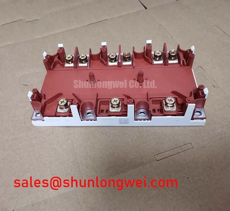
With the DC link isolated and discharged, I begin a service check at the main power terminals rather than at the gate driver. The SKIM401GD128D is identified by Semikron as a 1200.0 V, 400.0 A IGBT module in a Semitrans package. These are official specification values; they do not by themselves define the permissible switching current, thermal operating point, or suitability for every inverter topology.
For a bolted busbar joint, a four wire micro ohmmeter is the correct instrument for investigating contact quality. The test probes should be placed on the conductive terminal surfaces rather than across the bolt head and an adjacent painted or plated area. A measured value below 10 µΩ may be used as a site acceptance target only when that limit comes from the equipment maintenance procedure or connection design. It is a Design Consideration, not an official SKIM401GD128D specification supplied here. Record the ambient temperature, test current, probe locations, and fastening condition so that later measurements remain comparable.
Thermal imaging adds useful evidence when the module has been operating under load. Compare the temperature pattern at the positive and negative power connections, the busbar transition, and the cable or laminated conductor immediately outside the module. A localized hot area at one joint deserves mechanical inspection, while a broad temperature rise across the complete current path points toward system loading, cooling, or conductor layout. Inspect the joint after isolation for uneven washers, damaged plating, distorted busbars, oxide contamination, and evidence that the conductor has relaxed after vibration.
Keep the high current path compact and physically separated from sensitive gate and auxiliary emitter wiring. The purpose is to reduce stray inductance and prevent switching voltage from coupling into the control loop. Clearance and creepage must be selected from the complete DC link voltage, pollution environment, insulation system, and applicable equipment standard. A 1200.0 V module rating is not a substitute for a complete insulation coordination review in a central photovoltaic inverter.
For a replacement assessment, compare the terminal arrangement, mounting envelope, thermal interface, gate connections, and switching requirements before any power is applied. The neutral product page for SKM300GB12T4 can be reviewed as a related Semikron module reference, but its electrical and mechanical compatibility must be established by the system designer rather than assumed from the brand or package family.
⚠️ Field Alert: Disconnect the DC link and auxiliary supplies before removing busbars or control connectors, then follow the equipment manufacturer’s fastening procedure for the actual terminal hardware.
Preventing Spurious Faults: Auxiliary Emitter Pinout Cold Check Guidelines for SKIM401GD128D
The auxiliary emitter return must be treated as a dedicated driver reference, not as an interchangeable extension of the main load emitter connection. During a cold check, identify the power emitter and auxiliary emitter from the module marking and the original circuit documentation, then trace each conductor back to the driver board. Do not infer pin identity from connector position alone when a replacement harness or adapter has been installed.
With all sources isolated, check continuity from the driver return to the intended auxiliary emitter terminal and inspect for an unintended connection to the high current emitter path. A low resistance reading between terminals is not sufficient evidence of correct topology because semiconductor junctions, parallel copper paths, and protection components can influence a meter test. Use the wiring diagram and connector keying to confirm the actual route.
The gate driver loop should remain short, direct, and physically separated from the commutation path. This arrangement helps limit ground bounce caused by rapid current change in the power circuit. The driver reference should return to the auxiliary emitter point specified by the module documentation, while the main emitter connection should carry the load current independently. Final loop geometry, insulation spacing, and driver damping remain system Design Considerations that require testing on the assembled inverter.
False gate activity can also originate from poor isolation, a floating driver supply, damaged connector contacts, or excessive common mode voltage. Observe the gate to auxiliary emitter signal with a suitable differential probe during controlled bench testing. Compare the waveform with the driver supply behavior and the switching node at the same time. A pulse that appears only when the main power circuit commutates may indicate coupling or reference movement, but it should be confirmed against the known good signal path rather than assigned to one component immediately.
Vibration proofing is part of the electrical design. Support the harness so that the auxiliary emitter contact is not carrying cable weight, secure the busbar without imposing lateral force on the module terminals, and inspect crimp barrels for movement. Creepage and clearance around the control connector must account for the highest potential nearby, surface contamination, enclosure conditions, and service access. These spacing decisions are not established by the 400.0 A current rating.
Benchtop Waveform Tuning: Coordinating High Speed Arcing Voltage on SKIM401GD128D
Fuse coordination must be assessed as a complete interruption event. A semiconductor fuse selected for a high power inverter should be compared with the module’s short circuit capability, the DC link energy, the available fault current, and the fuse total clearing I²t. The fuse nameplate value alone does not prove that the module will remain within its electrical and mechanical stress limits during a fault.
On the bench, begin with a controlled low energy switching test and confirm probe bandwidth, grounding, and measurement loop area before interpreting overshoot. Measure the switch node, gate to auxiliary emitter voltage, and DC link behavior using equipment rated for the transient environment. Minimize measurement loop inductance because an unnecessarily long probe connection can create an apparent spike that is not present at the module terminal.
Fast arcing voltage during fuse interruption can couple into the gate circuit through stray capacitance and common impedance. The protection network should be evaluated as a coordinated system that may include a gate clamp, a suitable snubber, a metal oxide varistor, and the inverter’s upstream surge protection. The voltage rating, energy capability, pulse repetition, and failure mode of each protective component must be selected from the actual DC link and fault study. These are Engineering Recommendations for system development, not SKIM401GD128D factory specifications.
Long motor cables and large cabinet bus structures can create transmission line effects. Reflected voltage may combine with the original switching edge and produce a higher local peak at the module or motor terminals. Cable routing, termination, switching speed, output filtering, and motor insulation class should therefore be evaluated together. A filter should not be added by assumption; its impedance and damping must be checked against the inverter control loop and the intended switching frequency.
When integrating the module into a utility scale photovoltaic central inverter, designers should verify that the topology, DC link arrangement, surge environment, and switching test results remain compatible with the 1200.0 V voltage rating. A system described as a 1500 V photovoltaic installation may use internal voltage segmentation or another topology, but the compatibility decision belongs to the completed electrical design. The related Industrial Applications reference provides broader context for evaluating IGBT power stages in demanding energy equipment.
Transient Dynamics & Electrical Design: Isolated DC DC Power Supply Sizing for SKIM401GD128D
The isolated driver supply must be checked at the gate driver terminals under switching conditions, not only with a static multimeter reading. Confirm the required voltage, current, startup behavior, undervoltage lockout, isolation construction, and transient response from the driver and power supply documentation used in the equipment. The SKIM401GD128D rating does not specify the auxiliary supply voltage or the required gate drive waveform.
A reinforced galvanic isolation barrier is a Design Consideration where the driver crosses the high voltage domain. A barrier test level above 5 kV and common mode transient immunity above 100 kV/µs should only be treated as project requirements when they are defined by the selected isolated driver, converter, and applicable safety design. They are not official ratings stated for this module. The insulation system must also consider creepage, clearance, working voltage, pollution degree, altitude, and the construction of the PCB and transformer.
At startup, monitor the isolated supply, enable signal, gate output, and fault feedback together. A slow or uneven supply ramp can leave the driver in an indeterminate state, while inadequate decoupling can produce a gate pulse during a high current transition. Gate dead time should prevent simultaneous conduction in the applicable bridge leg, but the value is system determined by device switching behavior, driver delay, temperature, load current, and protection response. Validate it on the assembled power stage rather than copying a generic setting.
Keep the isolated supply loop compact and place its high frequency bypass components according to the driver manufacturer’s layout guidance. Separate primary and secondary copper according to the required insulation system, and prevent copper pours or mounting hardware from creating an unintended bridge across the isolation barrier. When evaluating Semikron power module technologies, the manufacturer’s information on Semikron MiniSKiiP® Power Modules and Semikron Sintering Technology should not be interpreted as confirmation of construction details for this specific Semitrans model.
Thermal assembly also affects electrical repeatability. The heatsink surface should be clean and flat, the thermal interface should be applied evenly, and the clamping method should distribute pressure across the module base without bending the package. Disc spring arrangements can help maintain pressure during thermal cycling when they are correctly selected for the actual fastener and assembly stack. Final pressure, torque, insulation, and thermal resistance must follow the module and equipment documentation, with temperature verified during a controlled load test.