


Content last revised on September 22, 2026
TT61N12KOF-L2 Key Specifications
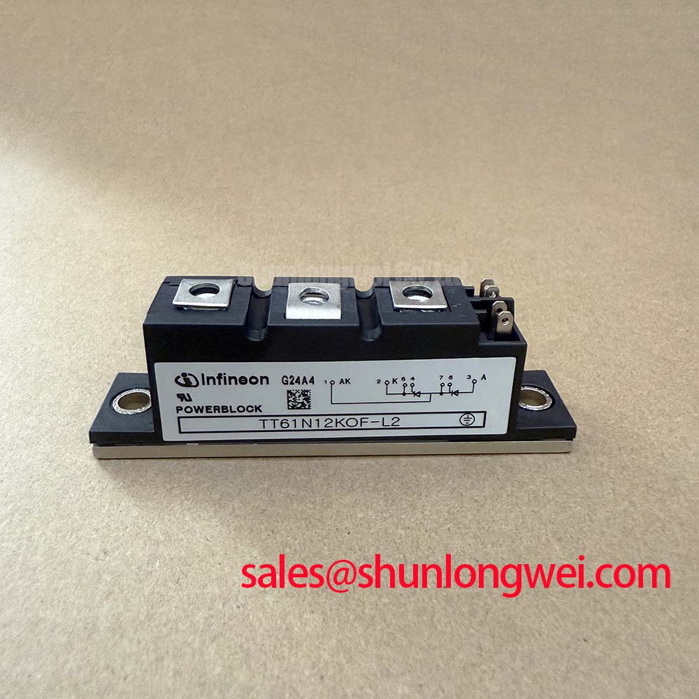
Check the module marking, terminal polarity, and any required cold-state resistance or continuity test before connecting the TT61N12KOF-L2 to a powered assembly. This Infineon dual thyristor module is specified with a 1200 V repetitive peak reverse voltage and 61 A average on-state current at TC = 85°C, making those ratings the first limits to compare with the rectifier’s electrical and cooling conditions.
| Official Specification | Value | Engineering Significance |
|---|---|---|
| Repetitive peak reverse voltage, VRRM | 1200 V | Defines the rated repetitive reverse-voltage boundary for circuit evaluation. |
| Average on-state current, ITAVM | 61 A at TC = 85°C | Applies under the stated case-temperature condition and cooling arrangement. |
| Junction-to-case thermal resistance, Rth(j-c) | Maximum 0.52 K/W per thyristor | Provides the official thermal path value for heatsink calculations. |
| On-state voltage, VT | Typical 1.25 V at IT = 150 A and Tvj = 25°C | Useful for estimating conduction loss at the stated test point. |
| Non-repetitive surge on-state current, ITSM | 1550 A at t = 10 ms and Tvj = 130°C | Describes short-duration surge capability under the specified test conditions. |
Benchtop Waveform Tuning: Short-Circuit Coordination for TT61N12KOF-L2
For a high-current green hydrogen electrolyzer DC power rectifier, begin short-circuit evaluation by comparing the selected semiconductor fuse clearing I²t with the thyristor module’s applicable coordination data. The 1550 A ITSM value is a non-repetitive surge rating, not a substitute for a fuse coordination table or a guaranteed short-circuit protection system. The fuse manufacturer’s pre-arcing and total-clearing data, prospective fault current, source impedance, and circuit time constant must be checked together.
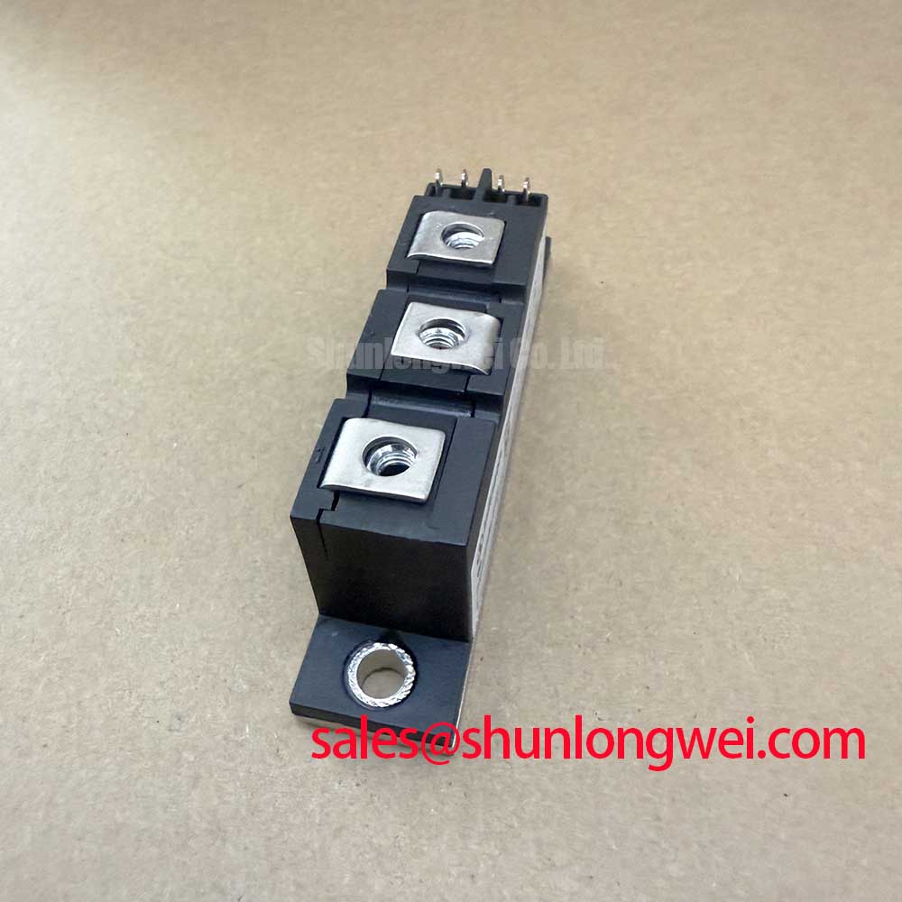
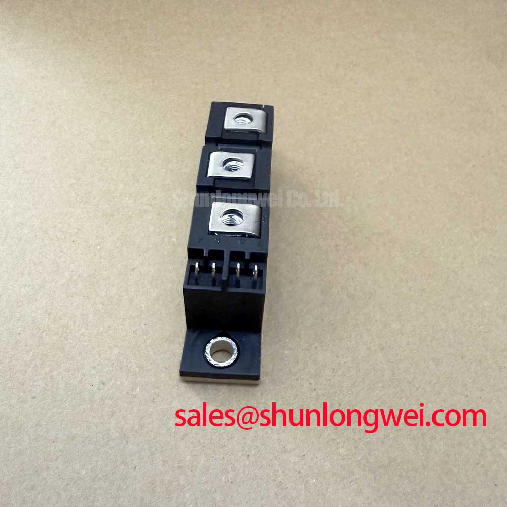
During bench work, record the actual terminal arrangement from the original assembly drawing and confirm that the replacement’s power terminals and gate connections correspond to the intended circuit. Do not infer an unused terminal function from physical position alone. The supplied product data does not state a mounting torque or fuse I²t coordination value, so those figures should be taken from the applicable Infineon mechanical documentation and the system manufacturer’s protection study.
⚡ Safety Interlock Note: Isolate and discharge the rectifier before removing terminals or taking resistance measurements.
Benchtop Waveform Tuning: Firing Angle, Harmonics, and Line Filtering
A dual thyristor module controls rectifier conduction through gate-trigger timing, so the firing-angle range must be evaluated against the electrolyzer power supply’s required DC output, displacement power factor, reactive power, and line-current distortion. The requested firing-angle sweep from 0° to 150° is a system-level test plan, not an official operating guarantee for this specific part. Engineers should measure line current and DC output under the actual transformer, commutation inductance, load, and controller conditions.
Line-filter selection should follow measured harmonic content rather than a generic component value. Verify that the filter does not interfere with commutation or create excessive transient voltage at the thyristor terminals. The module’s 1200 V VRRM rating is the official repetitive reverse-voltage limit; switching spikes and supply transients still require oscilloscope verification at the device terminals. Infineon’s material on .XT Technology and its OptiMOS™ product information concern other semiconductor technologies and should not be treated as specifications for this thyristor module.
Benchtop Waveform Tuning: Junction-to-Heatsink Heat Dissipation
Use the official maximum 0.52 K/W Rth(j-c) per thyristor as the starting point for the thermal path from silicon junction to case. The stated 61 A ITAVM at TC = 85°C is conditional on the specified case temperature and cooling environment; it should not be transferred directly to an arbitrary heatsink, airflow pattern, or enclosure.
Inspect the heatsink contact surface for burrs, contamination, and uneven pressure before installation. Apply the thermal interface material according to its supplier instructions and tighten the module using the mechanical specification applicable to this package. Confirm that the base remains seated without distortion, then monitor case temperature and both conducting paths during a representative load test. A thermal imbalance may indicate contact, current-sharing, wiring, or measurement issues and should be compared with a known-good assembly.
Preventing Spurious Faults During Rectifier Commutation
The TT61N12KOF-L2 is identified here as a dual thyristor module. The supplied official data does not provide diode reverse-recovery current, reverse-recovery time, Miller charge, active-clamp limits, or IGBT-style dead-time specifications. Those parameters must not be assigned to this device without the applicable datasheet. For commutation testing, capture anode-to-cathode voltage, load current, gate signal, and terminal ringing at the module pins while checking peak values against the rectifier’s DC-link and line-voltage boundaries.
Keep high-current and gate wiring physically separated where the equipment layout permits, and minimize the parasitic loop that can couple commutation noise into the trigger circuit. Gate pulse amplitude, pulse width, gate resistance, and any snubber network remain system-determined values requiring validation with the actual controller and load. For structured fault measurement and preventive checks, consult the Field Engineer’s Handbook. Engineers comparing package class or current capability may also review the TT570N16 as a separate reference device, subject to full electrical and mechanical compatibility checks.