


Content last revised on September 12, 2026
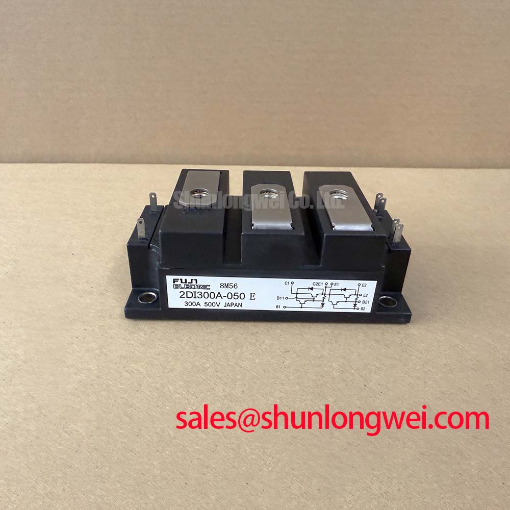
2DI300A-050 Thermal Electrical Optimization: Surge Energy Dissipation and Clamping Voltage Practical Tuning
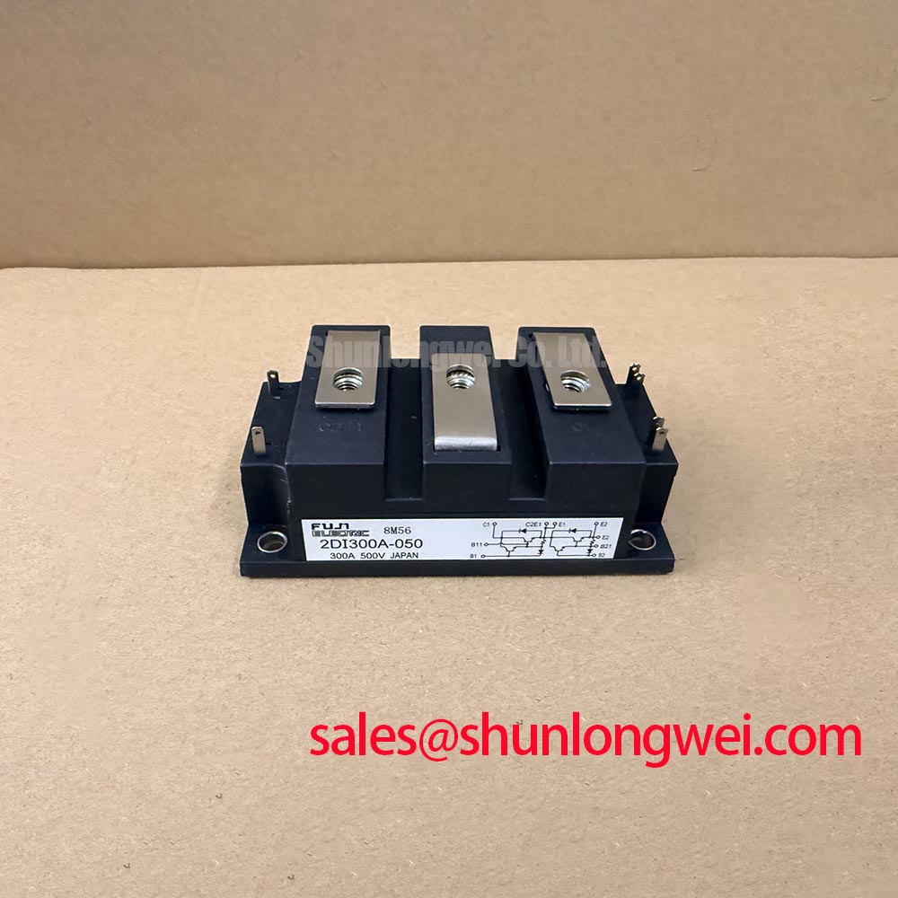
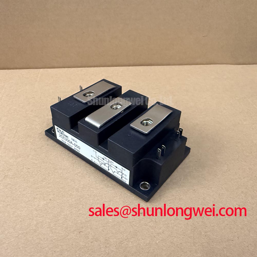
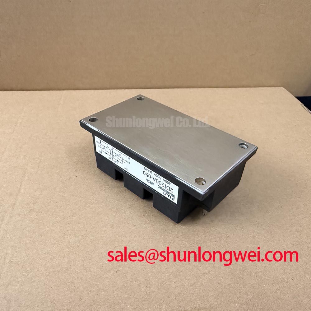
| Product | Fuji Electric 2DI300A-050 |
|---|---|
| Category | IGBT Module |
| Collector Emitter Voltage | 500 V VCES |
| Continuous Collector Current | 300 A IC |
| Gate Emitter Voltage | ±20 V VGES |
| Collector Emitter Saturation Voltage | 2.7 V maximum at 300 A and 125°C |
| Collector Cut Off Current | 1 mA maximum at 500 V |
| Thermal Resistance | 0.083°C/W maximum junction to case per IGBT |
| Operating Junction Temperature | −40°C to +150°C |
Measure the DC link and switching node with an isolated differential probe while checking the 2DI300A-050 against its 500 V VCES absolute maximum rating. This first waveform check should capture the overshoot produced when the rectifier or switching junction changes conduction state, rather than relying on a multimeter reading taken during steady operation.
For a high current green hydrogen electrolyzer DC power rectifier, the upstream protection network may include metal oxide varistors and an RC snubber stage. This is a system level design consideration, not a factory parameter of the module. The MOV clamping level, energy capability, fuse coordination, and snubber damping must be selected from the actual AC input, prospective fault current, wiring inductance, and repetitive surge profile. IEEE 61000 4 5 testing can provide a useful immunity framework, but it does not establish a standalone compliance claim for this power module.
Check each main terminal for clean contact, correct polarity, and stable mechanical seating. The supplied factory data does not define a terminal torque value or a fuse I²t coordination table, so those values should be taken from the applicable Fuji Electric installation documentation and the selected fuse manufacturer. The module’s 0.083°C/W maximum junction to case thermal resistance per IGBT provides a thermal calculation input; heatsink performance, interface condition, airflow, and switching duty remain system dependent.
When the switching waveform approaches the voltage boundary, compare the measured peak under cold and fully warmed conditions. Engineers evaluating a related device can review 2DI100D-100 as a separate same family reference, while retaining the original electrical and mechanical qualification for this model.
Assembly Integrity and Layout Architecture: Implementing Reverse Recovery Charge for 2DI300A-050
Capture the commutation interval at the module terminals with a short, properly arranged probe connection and compare forward current, reverse current, and voltage recovery on a known good assembly. The supplied factory data does not specify diode reverse recovery peak current Irrm, reverse recovery time trr, or soft recovery behavior, so these characteristics must not be inferred from the 300 A continuous collector current rating.
Reverse recovery behavior affects commutation loss, voltage overshoot, and radiated noise. A practical layout consideration is to keep the high current commutation loop compact and to separate gate drive return paths from the power return path. The final arrangement should be validated with oscilloscope measurements at the intended current, temperature, and switching frequency. A bootstrap capacitor and its charging diode also require system verification for high frequency operation; capacitance, ripple current, dielectric rating, and recovery behavior are determined by the driver topology.
The gate emitter rating is ±20 V VGES as an official specification. Gate voltage should therefore be monitored directly at the module terminals, including transient behavior during turn off. Common mode transient immunity of an optocoupler or digital isolator belongs to the driver and control board design. Verify isolation layout, return current paths, and switching waveforms against the selected isolator documentation rather than assigning a CMTI value to the module.
For upstream rectification coordination, the neutral reference 2DI100Z-120 may be reviewed as a separate complementary stage. It is not an automatic substitute, and voltage, current, mounting, and circuit topology must be checked independently.
Assembly Integrity and Layout Architecture: Mitigating DC Ripple Currents in High Efficiency Rectifiers
Inspect the DC output with a differential probe and current probe at the rectifier terminals, then compare ripple current between parallel paths before changing the control settings. The 2DI300A-050 is specified for 300 A continuous collector current; this rating does not by itself confirm suitability for a particular six pulse or twelve pulse bridge, transformer arrangement, or parallel module bank.
A six pulse bridge can be evaluated for a simpler rectifier topology, while a twelve pulse arrangement may reduce characteristic ripple when the transformer phase displacement and interphase transformer are correctly coordinated. These are engineering recommendations for system evaluation. Transformer leakage, busbar resistance, semiconductor forward voltage, thermal gradients, and gate timing can produce unequal static or dynamic current sharing between parallel paths.
Use matched conductor geometry and symmetrical busbar paths where parallel operation is being considered. Confirm current sharing at startup, rated output, current transitions, and thermal steady state. The official electrical characteristic lists 2.7 V maximum VCE(sat) at IC = 300 A and Tj = 125°C. Because this value is specified under a defined test condition, it should be used with the actual loss model and junction temperature measurement rather than treated as a universal operating voltage.
In electrolyzer rectifier service, inspect the interphase transformer, DC link capacitor connections, and terminal temperature together. ⚠️ Maintenance Note: Monitor contact temperature during scheduled service and remove dust or airflow restrictions before tightening connections. Moisture and condensation control also matters in cold industrial enclosures; allow the assembly to reach a stable dry condition before applying high voltage.
Benchtop Waveform Tuning: Mitigating Stress Through Repetitive Surge Evaluation
Record the peak current and case temperature during the prescribed surge test, then allow the assembly to return to its defined thermal condition before applying reverse voltage again. The supplied factory data does not state an ITSM sinusoidal 10 ms half cycle surge rating, so no repetitive surge limit can be assigned to this model from the listed parameters.
Use the official operating junction temperature range of −40°C to +150°C as the documented boundary for evaluation, while recognizing that repetitive surge capability depends on pulse duration, initial junction temperature, cooling path, repetition rate, and circuit impedance. Fuse clearing behavior and the selected fuse I²t must be coordinated from documented device and fuse data.
During bench tuning, verify that the measured VCES peak remains within the 500 V collector emitter voltage rating under the worst switching condition. Review the The Ultimate IGBT Knowledge Base for broader IGBT measurement principles, and consult Fuji Electric Europe Semiconductor and Power Electronics for manufacturer level semiconductor information.