
Content last revised on September 10, 2026
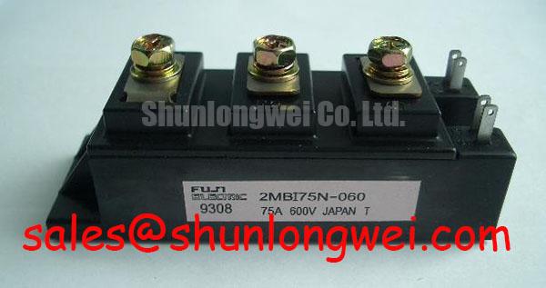
Incoming Bench Evaluation & Specifications for the 2MBI75N-060
In power electronics remanufacturing and incoming quality assurance, verifying half-bridge power modules requires rigorous static parameter verification before integration into material handling drive stages. The 2MBI75N-060 manufactured by Fuji Electric is a dual-pack (half-bridge) N-channel IGBT module engineered for motor drive inverters, uninterruptible power supplies (UPS), and low-voltage industrial traction systems. Operating across material handling platforms such as electric pallet jacks, reach trucks, and warehouse tuggers, this module provides symmetrical switching branches designed to handle moderate current density with low thermal impedance.
Static characterization on the bench begins with verifying channel isolation and the forward conduction state of the anti-parallel freewheeling diodes. Technicians must validate low-current collector-emitter breakdown, gate-to-emitter threshold uniformity, and baseplate isolation voltage before mounting assemblies to liquid or forced-air heatsinks.
| Parameter | Official Datasheet Specification | Bench Measurement Condition |
|---|---|---|
| Collector-Emitter Voltage (VCES) | 600V | VGE = 0V, IC = 1mA, Tj = 25°C |
| Continuous Collector Current (IC) | 75A | Continuous DC, TC = 25°C |
| Collector-Emitter Saturation Voltage (VCE(sat)) | Typical 2.1V (Max 2.7V) | IC = 75A, VGE = 15V, Tj = 25°C |
| Maximum Power Dissipation (Ptot) | 310W | Per IGBT element, TC = 25°C |
| Operating Junction Temperature (Tj) | -40°C to +150°C | Continuous operational range |
| Isolation Voltage (Visol) | 2500V AC | AC 1 minute, all terminals to baseplate |
💡 Bench Tip: When performing static diode checks across terminals C1-E1 and C2-E2/E1 with a digital multimeter on diode range, expect a cold-state forward drop between 0.38V and 0.52V at standard room temperature (25°C) across the internal fast-recovery diodes (FWD). Always short the gate-emitter terminals (G1-E1 and G2-E2) with conductive foam or an ESD clip during handling to prevent electrostatic discharge from puncturing the sensitive SiO2 gate dielectric layer.
Thermal Feedback & V_CE(sat) Positive Temperature Coefficient Equalization
In electric forklift and reach truck traction systems, inverters often operate under severe low-speed, high-torque conditions where current peaks stress single legs of a multi-phase bridge. When evaluating the 2MBI75N-060 for current distribution consistency, the temperature dependency of the collector-emitter saturation voltage VCE(sat) is a critical physical mechanism. At nominal operational current levels (IC = 75A), the module exhibits a slightly positive temperature coefficient at higher current regimes, where an increase in junction temperature results in a moderate increase in VCE(sat).
This positive coefficient acts as an intrinsic thermal stabilization feedback loop. When one IGBT die within a parallel-branch arrangement experiences localized heating due to thermal interface resistance unevenness, its internal conduction resistance rises, naturally shifting incremental current to cooler, lower-impedance paths. During incoming QA screening, technician teams record VCE(sat) across paired modules under pulsed high-current conditions (100 µs pulse width to prevent self-heating) to ensure matched forward drops within a +/- 50mV window.
For systems requiring higher current handling without paralleling discrete modules, the related 2MBI300J-060 offers a continuous 300A rating at 600V VCES within a larger mechanical footprint. Maintaining symmetrical busbar geometry and matched external gate loop trace lengths is critical to avoid dynamic switching imbalance during microsecond-level turn-on transitions.
Thermal Cycling Margins of Internal Braking IGBTs under Repetitive Stop-Start Duty
Electric material handling equipment undergoes severe duty cycles characterized by rapid acceleration, continuous mechanical plugging, and active regenerative braking. During decelerations, kinetic energy from the traction motor feeds back into the DC link bus capacitors. When battery chemistry or state-of-charge limits reverse absorption, dynamic brake chopper stages direct excess energy into high-power ballast resistors.
Dynamic braking puts severe thermal cycling stress on internal bonding wires and substrate solder joints. When the braking IGBT switches high pulsed current into resistive banks, junction temperature swings (ΔTj) can exceed 60°C within fractions of a second. To calculate the bootstrap circuit sizing for driving the high-side switch during extended deceleration periods, engineers must account for the total gate charge Qg and the quiescent current drawn by the isolated gate driver IC, ensuring the high-side floating supply rail does not drop below the undervoltage lockout (UVLO) threshold.
Consulting technical architectures outlined on the Fuji Electric Brake Chopper IGBT Modules engineering portal confirms the necessity of thermal derating under high-frequency braking duty. Heatsink mounting torque must be kept strictly within 2.5 to 3.5 N·m using calibrated M5 hardware, combined with a uniform thermal grease layer of 50 to 80 µm to prevent void-induced hot spots during repetitive kinetic energy absorption cycles.
Optocoupler vs Digital Coreless Transformer Isolation in High-Voltage Switching
Galvanic isolation integrity is critical in industrial motor drives to separate the high-voltage DC bus (typically 48V to 380V in material handling systems) from low-voltage microcontrollers and DSP boards. Two isolation topologies dominate gate drive circuitry: traditional optocouplers and digital coreless transformer isolators. The primary vulnerability in high-speed IGBT switching environments is high common-mode transient dv/dt generated across the phase node during hard turn-off transitions.
When the collector-emitter voltage swings rapidly, displacement currents cross the isolation barrier parasitic capacitance (Ciso). Optocouplers with inadequate Common-Mode Transient Immunity (CMTI < 15 kV/µs) risk parasitic logic state toggling, causing unintended gate firing and catastrophic DC bus shoot-through. Digital coreless transformer isolators provide CMTI figures exceeding 100 kV/µs along with higher reinforced isolation barriers (>5 kV), offering robust immunity against rapid voltage slew rates.
In accordance with testing procedures detailed in the Field Engineer’s Handbook, bench technicians verifying field returns must perform hi-pot leakage testing between power terminals (C1, C2, E1, E2) and the electrically isolated copper baseplate. The Fuji Electric 2MBI75N-060 provides a factory-tested 2500V AC isolation barrier for 60 seconds (Official Datasheet Specification). Any degradation in insulation resistance below 100 MΩ at 1000V DC indicates ceramic substrate micro-cracking caused by mechanical shock or excessive mounting warping.
Auxiliary Emitter Return Trace Separation for Rapid dv/dt Transients
A frequent failure mechanism identified during bench analysis is uncontrolled oscillation or parasitic turn-on induced by shared emitter inductance. The 2MBI75N-060 physical pinout provides dedicated auxiliary Kelvin emitter terminals separate from the main high-current power emitter connections. The high di/dt generated during hard turn-off transitions across stray inductance in the high-current path generates an induced counter-electromotive voltage that opposes the driver turn-off signal if the gate return is tied directly to the power emitter busbar.
Separating the signal emitter return trace directly from the auxiliary Kelvin pin back to the gate driver decoupling capacitor isolates the low-voltage gate loop from the high di/dt power path. This design practice prevents mutual inductive coupling from corrupting the gate signal. Layout clearances should maintain at least 4.0 mm clearance and 6.3 mm creepage distances across high-voltage traces on printed circuit boards.
For detailed design specifications and footprint drawings across diverse dual-pack configurations, refer to the Fuji Electric Power Semiconductors Portal. When scoping gate waveforms on the test bench, differential probes should connect directly across the module's auxiliary gate and emitter pins to verify that turn-off negative gate damping prevents Miller clamp threshold breaches during rapid inductive load commutations.