


Content last revised on September 10, 2026
6MBI75U2A-060 Circuit Protection & Reliability: Calibrating Thermal Interface Material Thickness Uniformity
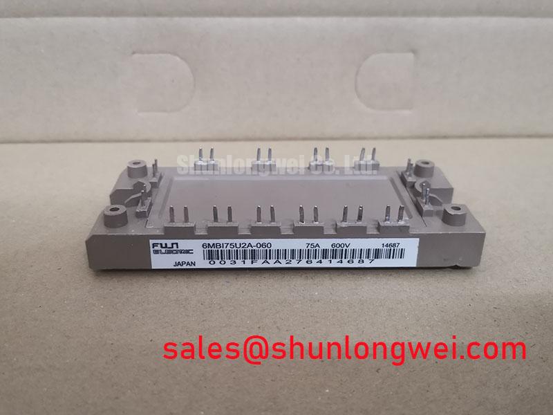
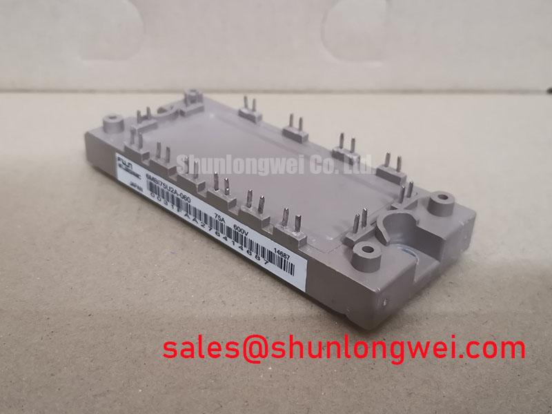
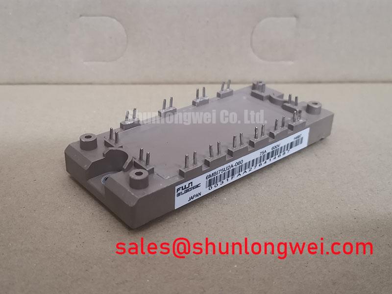
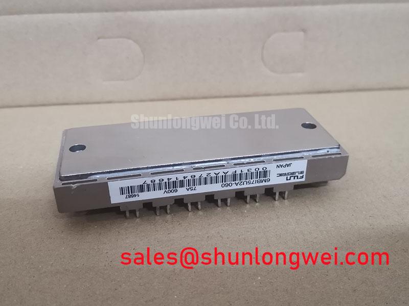
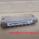
Begin incoming inspection by checking the Fuji Electric 6MBI75U2A-060 marking, module body, terminal condition, and mounting base under controlled ESD handling. The official product data supplied for this device identifies a 600.0 V voltage rating, a 75.0 A current rating, and a Module package. These values establish the initial identity and application boundary; they do not replace the complete manufacturer datasheet or the thermal design limits of the converter.
Before applying power, record the cold state of the accessible terminals and compare the readings with a known good reference unit or the original maintenance record. A diode test across the appropriate freewheel paths can help confirm junction polarity, but the measured forward voltage is influenced by the meter current, junction temperature, contact resistance, and the exact internal circuit path. It should therefore be treated as an incoming comparison measurement rather than a universal pass or fail threshold.
💡 Bench Tip: Use an ESD controlled bench, short the gate control terminals only according to the manufacturer’s handling guidance, and preserve a cold reference record before connecting the module to a powered test fixture.
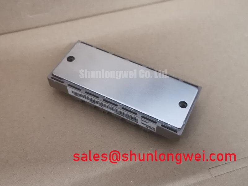
Thermal installation requires a flat, clean interface between the module base and heatsink. A thermal interface material should be applied as a controlled, continuous layer rather than as isolated pads or excessive compound. The correct thickness is a Design Consideration governed by the material supplier, surface flatness, baseplate condition, clamping method, and required thermal resistance. Excess material can increase thermal resistance and migrate toward terminals, while insufficient coverage can leave air pockets beneath the baseplate.
Inspect the mating surfaces for burrs, contamination, foreign particles, and visible curvature. If the module or heatsink has measurable bowing, the engineering team should determine whether the assembly needs surface correction, a qualified interface pad, or a different clamping arrangement. Do not attempt to compensate for substantial curvature by tightening one corner first, since local pressure can distort contact and place mechanical stress on the package.
Use a crosswise or sequential tightening pattern so that the baseplate settles evenly. The fastening torque must come from the relevant Fuji Electric mechanical specification, the fastener grade, and the heatsink assembly drawing. A general M5 torque value is not automatically an official parameter for this model. After installation, inspect the interface perimeter and confirm that the heatsink remains mechanically stable without forcing the module body.
For a commercial string inverter or microgrid energy storage converter, keep high current paths short and physically separated from low level gate control wiring. Clearance around power terminals should be established from the system voltage, pollution environment, insulation system, and applicable safety standard. Creepage and clearance are system insulation decisions, not package ratings that can be inferred from the 600 V designation alone.
When a thermal alarm appears during commissioning, check the complete heat path before attributing the result to the IGBT. Review fan or liquid cooling operation, heatsink flatness, interface coverage, busbar torque, phase current balance, switching frequency, and temperature sensor placement. Compare phase waveforms and case temperature under the same load conditions. A difference between phases may indicate an assembly, gate drive, current sharing, or measurement issue and should be confirmed with controlled instrumentation.
6MBI75U2A-060 Operational Boundaries: Evaluating Dynamic Gate Impedance Control for Robust Limits
Gate circuit inspection should start at the module terminals and continue back to the driver output, return path, isolation barrier, and control ground. The purpose is to identify unwanted common impedance, long parallel runs, and coupling from the collector or emitter power path. The 6MBI75U2A-060 official ratings do not by themselves define a universal gate resistor, gate voltage, switching speed, or negative off bias. Those values must be selected from the applicable Fuji Electric electrical characteristics and verified against the actual driver and layout.
A Design Consideration for fast inverter legs is to minimize parasitic gate loop inductance and keep the turn on and turn off paths predictable. When a complementary device switches, collector voltage movement can capacitively couple into the inactive gate. A dedicated active Miller clamp can reduce the impact of this coupling when the driver architecture, clamp threshold, propagation delay, and layout are compatible. The control engineer should validate the result with a differential probe at the module gate terminals, not only at the driver board connector.
Negative gate bias is sometimes evaluated to increase off state noise immunity in high dv/dt bridges. The requested range of negative bias must not be treated as a default prescription for this module. It is an Engineering Recommendation only when supported by the manufacturer’s gate limits, driver isolation design, turn off behavior, and fault response. Excessive negative bias can create its own stress and must be checked during startup, shutdown, short circuit, and abnormal commutation tests.
For phase angle control, confirm that the commanded duty pattern reaches the intended power devices without overlap caused by propagation delay or ground movement. Observe both gate to emitter voltages and the corresponding collector emitter transitions. A gate waveform that appears correct at the driver output can differ at the module because of wiring inductance and common emitter voltage movement. If the module provides a separate auxiliary emitter connection in the relevant configuration, its routing should be kept distinct from the high current emitter return, subject to the actual terminal diagram.
Line frequency ripple smoothing belongs to the DC link and control system rather than to the module alone. In a commercial photovoltaic inverter or battery energy storage converter, designers should evaluate capacitor ripple current, control loop response, modulation behavior, and busbar inductance together. The 6MBI75U2A-060 should be exposed to voltage and current conditions that remain within the complete Fuji Electric operating limits after switching overshoot and ripple have been measured.
RC snubber selection is also system determined. A snubber can reduce ringing when its impedance, placement, pulse energy capability, and parasitic inductance are appropriate, but an incorrectly placed network may increase loss or fail to control the dominant loop. Measure the collector emitter waveform at the module terminals during representative switching events. Fuji Electric application material, including its information on Fuji Electric Brake Chopper IGBT Modules, provides useful manufacturer context for evaluating switching and protection behavior, while the exact limits must be taken from the applicable device documentation.
6MBI75U2A-060 Operational Boundaries: Evaluating High Speed Fault Management: VCE Desaturation Limits
Desaturation protection should be assessed as a complete fault chain: current rise, voltage sensing, blanking behavior, gate shutdown, isolation delay, fault latch, and controller response. The 6MBI75U2A-060 product identity and ratings do not establish a universal desaturation threshold or a guaranteed short circuit withstand time. Any claimed short circuit safe operating area must be taken from the relevant Fuji Electric datasheet or application document for the exact revision and test conditions.
A practical Engineering Recommendation is to verify the fault detector using a controlled low energy test fixture before connecting the full DC link. Confirm that the sensing path responds to a genuine high VCE condition while remaining stable during normal switching transients. The test should include gate driver supply variation, temperature variation, expected diode recovery behavior, and the actual isolation interface. A false trip can arise from layout coupling or an unsuitable blanking arrangement, while a delayed trip can allow excessive semiconductor stress.
Some gate driver systems describe Type I and Type II short circuit responses, with the second stage applying a slower or shaped turn off after the initial fault decision. The exact timing, current reduction profile, and permitted pulse duration are application dependent. Do not present a sub ten microsecond response as an official characteristic unless it is explicitly stated in the Fuji Electric documentation for this part. The protection engineer should measure the delay from fault inception to gate action and compare the complete switching transient with the specified short circuit conditions.
Two stage soft turn off is intended to limit the di/dt associated with abruptly interrupting a high fault current. Its success depends on the driver output impedance, gate loop inductance, DC link stray inductance, clamp network, and fault location. During validation, record gate emitter voltage, collector emitter voltage, phase current, driver supply, and fault output on a common time base. Peak voltage must be checked against the system DC link and the device’s documented switching limits.
Fault troubleshooting should begin with a de energized inspection of the desaturation diode, sensing resistor network, blanking capacitor, driver ground, and fault latch. Next, compare the suspect channel with a known good channel using identical probes and grounding methods. If the fault signal is present without an abnormal power waveform, investigate noise injection and reference movement. If the power waveform is abnormal but the fault signal is absent, trace the sensing path from the module collector connection to the driver input without assuming a single failed component.
Gate turn off interference can be reduced by separating power commutation loops from the desaturation and fault signal wiring. The appropriate isolation distance is determined by the system insulation coordination and working voltage. Engineers evaluating off state noise behavior may also consult Evolution of Negative Off Bias Gate Drive Circuits as a technical reference, while choosing the actual gate bias and protection sequence from the module and driver documentation.
For broader topology review, the manufacturer’s Fuji Electric 7th Gen X Series IGBT Modules information can help distinguish general switching concepts from data specific to this product. The integrator should not transfer ratings, short circuit times, or protection recommendations from another series without checking electrical and mechanical compatibility.
6MBI75U2A-060 Thermal Electrical Optimization: Symmetrical Busbar Geometry for High Current Practical Tuning
At incoming inspection, confirm that the power terminals are clean, mechanically undamaged, and identified against the original circuit drawing before attaching busbars. The module’s official 75.0 A rating is a product specification, but usable current in an inverter depends on case temperature, switching conditions, duty cycle, cooling, overload profile, parallel path impedance, and the manufacturer’s derating information.
Symmetrical busbar geometry can help reduce differences in stray inductance between parallel or complementary current paths. Keep the forward and return conductors close enough to reduce loop area while maintaining the insulation clearances required by the system. Avoid routing a high current busbar directly over sensitive gate or desaturation wiring. If a laminated bus structure is used, validate its dielectric system, fastening method, thermal expansion, and fault withstand separately from the IGBT module.
At sufficiently high current density, the positive temperature coefficient of VCE(sat) is commonly considered when evaluating static current sharing at elevated temperature. This principle does not guarantee equal sharing in every assembly, because dynamic switching imbalance, unequal gate resistance, emitter wiring, thermal gradients, and measurement error can dominate. Measure each phase current and module case temperature under the intended modulation pattern, then compare turn on and turn off waveforms at the device terminals.
Gate loop symmetry is especially important where multiple devices or multiple phase legs are arranged beside one another. Use matched routing principles for gate and emitter return paths, keep driver reference connections separate from high current return conductors, and avoid unnecessary connector transitions. If a separate auxiliary emitter terminal is present on the actual module drawing, connect it only as specified and prevent its signal return from carrying load current. The terminal arrangement must be confirmed from the original Fuji Electric documentation rather than inferred from package appearance.
In a commercial string inverter or microgrid energy storage system, inspect the interaction between the IGBT bridge, boost stage, DC link, brake path, and upstream rectification or auxiliary conversion stage. A related device such as 6MBI300U-120 may appear elsewhere in a power topology, but its electrical rating and mechanical arrangement must be evaluated independently. It should not be treated as an automatic substitute or companion for the 6MBI75U2A-060.
When an engineer evaluates an alternative module, comparison should cover voltage class, current definition, switching and short circuit data, internal circuit topology, terminal layout, baseplate dimensions, isolation characteristics, gate limits, thermal resistance, and documented mounting requirements. The 2MBI150UC-120 can be reviewed as a separate candidate in a replacement study, but it is not a direct replacement unless the original equipment documentation and a complete electrical and mechanical verification confirm compatibility.
Finally, investigate unequal current by measuring the complete path rather than relying on visual symmetry alone. Check busbar contact pressure, terminal resistance, driver timing, gate emitter ringing, diode recovery, DC link ripple, thermal interface contact, and sensor calibration. Any change should be validated first at controlled energy, then under the intended operating envelope with oscilloscope records and temperature monitoring retained as part of the equipment repair file.