Content last revised on October 19, 2026
1DI300Z-140 Thermal-Electrical Optimization: Gate Drive Resistance Calibration and Practical Tuning
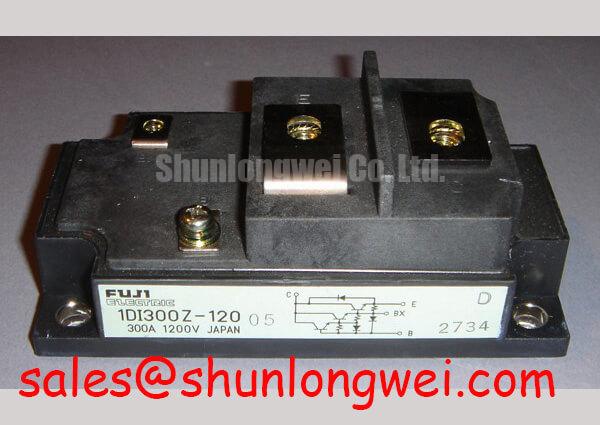
1DI300Z-140 from Fuji Electric is identified by an official rated voltage of 1400.0 V, an official rated current of 300.0 A, and a Power Transistor Module package. These are the primary product specifications for procurement and equipment replacement assessment. Gate-drive behavior, switching frequency, thermal impedance curves, terminal configuration, and installation requirements should be matched against the applicable device documentation before energizing a repaired heavy-duty variable frequency AC motor drive.
| Parameter | Specification |
|---|---|
| Manufacturer | Fuji Electric |
| Model | 1DI300Z-140 |
| Rated voltage | 1400.0 V, Official Specification |
| Rated current | 300.0 A, Official Specification |
| Package | Power Transistor Module, Official Specification |
- Confirm the cold-state terminal condition with the drive isolated and discharged.
- Inspect the mounting interface, heatsink contact area, and thermal compound condition before installation.
- Check gate-drive isolation, connector seating, and the return path for unwanted common-mode noise.
- Compare the replacement device ratings with the original drive protection and braking circuit.
When a modern replacement is fitted to a legacy drive board, adjust the external turn-on and turn-off gate resistance as a switching calibration task rather than copying the resistor arrangement without measurement. The correct balance depends on the driver capability, gate charge behavior, collector current, DC-link condition, wiring inductance, and the switching waveform observed at the module terminals.
A practical commissioning sequence begins with a low-energy switching check and a differential probe placed directly across the gate-emitter connection. Review turn-on delay, turn-off delay, voltage overshoot, ringing, and the relationship between gate waveform and collector current. If the turn-on path is too aggressive, switching stress and radiated disturbance may increase; if it is too slow, the device may spend longer in its linear transition. Turn-off resistance must be evaluated separately because the desired damping and current commutation behavior can differ from turn-on performance.
Design Consideration: keep the gate-drive loop compact, route the command and return conductors together, and separate high-current commutation paths from sensitive control wiring. A negative turn-off bias can be considered only when the driver, isolation arrangement, and module documentation support it. The final bias and resistor values are system-determined and require oscilloscope verification under the actual motor-drive operating conditions.
For a board-level replacement review, engineers may also compare the mechanical and electrical interface with 6DI50AH-050 as a separate device reference, not as an automatic substitute. Pin identity, voltage class, current behavior, mounting arrangement, and gate-drive compatibility must be checked independently.
Preventing Spurious Faults: Dynamic Power Loss Dissipation and Multi-RC Guidelines for 1DI300Z-140
Transient thermal evaluation should combine the module’s switching loss, conduction loss, overload duration, case temperature, and the applicable junction-to-case thermal response. A multi-RC thermal model is useful because a short braking pulse and a prolonged regenerative event do not stress the semiconductor in the same way. The calculated junction temperature should be compared with the documented transient thermal impedance curve and the system trip thresholds during the complete operating cycle.
Regenerative braking and large braking resistors can impose repeated pulsed loading on a variable frequency drive. Record the DC-link waveform, braking command, pulse duration, and heatsink temperature during controlled tests. A rising case temperature can also reflect blocked airflow, aged thermal interface material, uneven clamping pressure, or contamination on the heatsink. Inspect both sides of the thermal interface where the mechanical design uses double-sided cooling or a pressure-mounted arrangement.
Busbar geometry directly affects turn-off overshoot. Minimize the commutation loop area, use a laminated or closely coupled bus structure where practical, and place the snubber film capacitor at the switching loop rather than remotely on the cabinet backplane. The engineering target is to contain parasitic inductance sufficiently to suppress transient spikes, with the final layout verified by measuring the peak voltage at the module terminals. The IGBT Design & Integration reference provides additional guidance for gate-drive, thermal, and switching-layout evaluation.
⚠️ Maintenance Note: monitor contact temperature during scheduled service and recheck the heatsink airflow after cleaning, because thermal-interface aging and restricted ventilation can change the operating margin without changing the nominal load.
Material selection and mechanical pressure also deserve attention during overhaul. Use the specified mounting arrangement, inspect the heatsink for flatness and contamination, and tighten fasteners in a controlled sequence. Where a disc-spring pressure system is used, verify the intended pressure calibration from the equipment design rather than applying an assumed torque value. The external package does not by itself establish the complete thermal path.
1DI300Z-140 Circuit Protection & Reliability: High-Speed Protection Coordination
Protection coordination should start with the semiconductor fuse clearing characteristic and the module’s documented short-circuit or overload withstand capability. Compare the fuse total clearing I²t with the energy that can reach the power transistor during a DC-link fault, including wiring impedance, capacitor discharge, and the response delay of the drive protection circuit. Fuse selection based only on continuous current can leave the switching device exposed during the first fault transient.
During service testing, inspect the DC-link discharge path, fuse holder condition, busbar spacing, and the physical route between the protection device and the module. Arcing voltage and stray inductance can raise the local stress even when the measured cabinet voltage appears acceptable. Keep high-energy conductors firmly supported, maintain the clearance and creepage specified by the equipment design, and verify that snubber and clamp components are connected at their intended electrical nodes.
Protection validation should use controlled test conditions with voltage probes and current measurement appropriate to the DC-link energy. Observe whether the gate driver reports a fault before the protection fuse clears, and check for repeated nuisance trips caused by noise, desaturation timing, braking transients, or insufficient gate isolation. The 1400.0 V rating and 300.0 A rating are official product values, but the safe operating boundary in a complete drive remains dependent on switching conditions, cooling, protection coordination, and the documented application circuit.