



Content last revised on September 17, 2026
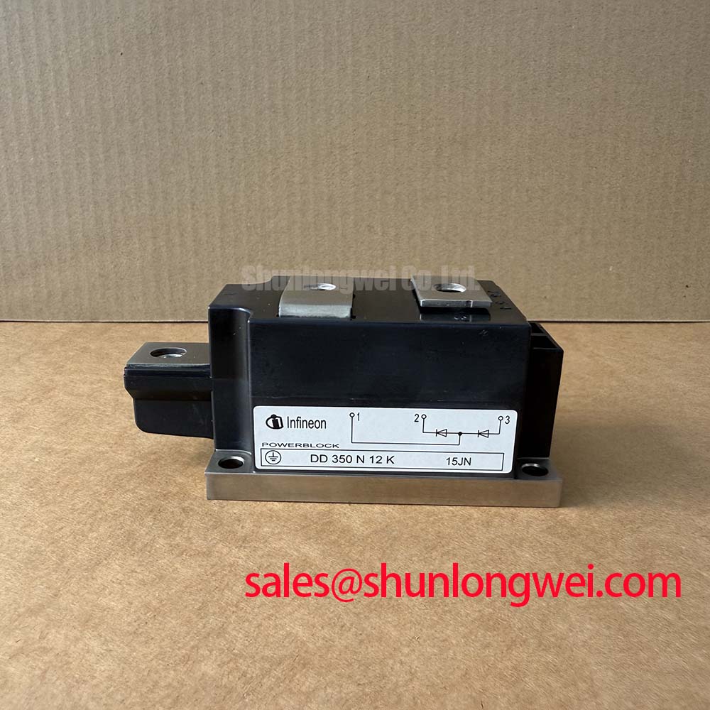
DD350N12K Circuit Protection & Reliability: Calibrating IEC 61000−4−5 Industrial Surge Immunity
The first protection review starts at the AC input and DC link rather than at the diode module alone. The commonly referenced surge immunity standard is IEC 61000−4−5; system conformance belongs to the completed equipment, not to an individual diode module. The DD350N12K rating of VRRM = 1200 V is the official repetitive reverse voltage limit. A design team should compare measured and simulated reverse voltage peaks at the module terminals against this limit under normal switching, supply disturbance, and controlled fault test conditions.
Metal oxide varistors, line impedance, RC suppression, contactor behavior, capacitor bank switching, and cable routing all influence the voltage presented to a rectifier position. As a Design Consideration, protection components should be selected from measured surge conditions and the equipment insulation architecture, with their energy capability and end of life behavior reviewed at the system level. It is not appropriate to infer an IEC surge performance class from the DD350N12K voltage rating alone.
Fuse coordination deserves the same evidence based treatment. The module’s 10,500 A, 10 ms IFSM specification describes a specified surge capability, while semiconductor fuse selection requires the fuse manufacturer’s time current and let through I²t information, the available prospective fault current, and the protected circuit topology. The supplied DD350N12K information does not state a module I²t limit, so an exact fuse I²t coordination table should not be created from the surge current figure. Maintenance teams should retain the original fuse data, inspect fuse holders and busbar joints for heat discoloration, and verify that the replacement path has not altered the intended fault clearing sequence.
| Verification item | Recorded value | Status |
|---|---|---|
| Reverse voltage rating | 1200 V Official Datasheet Specification | Compare with measured terminal stress |
| Average current rating | 350 A at case temperature of 100°C Official Datasheet Specification | Compare with thermal duty calculation |
| Surge current rating | 10,500 A for 10 ms Official Datasheet Specification | Review with original protection documentation |
| Fuse evidence | System determined | Use fuse manufacturer coordination curves |
Where an upstream rectifier or auxiliary power stage is also under review, the DDB6U180N16RRP_B37 page provides a separate reference point for documenting the device family and ratings actually installed. It should not be treated as a direct substitute without checking the complete electrical and mechanical interface.
Transient Dynamics & Electrical Design: RC Snubber Network Optimization to Prevent Transient Stress on DD350N12K
RC snubber evaluation should begin with an oscilloscope measurement directly across the relevant power terminals using a method appropriate for high voltage differential measurement. The objective is to identify the real ringing frequency, peak reverse stress, and repeatability across operating states. A sharp peak may be associated with busbar loop inductance, capacitor placement, switching behavior elsewhere in the topology, probe setup, or a combination of these factors. It should not be attributed automatically to the DD350N12K.
As a Design Consideration, minimize parasitic loop inductance between the commutating power path, the DC link capacitance, and the diode module where this reduces inductive overshoot. A stacked busbar arrangement can support this aim when it matches the established equipment geometry. The system engineer should validate peak voltage margin against DC link voltage during switching tests after any change to busbars, snubber parts, capacitor location, or wiring length.
RC snubber component values are system determined. They should be derived from the observed transient response, allowable power dissipation, switching repetition, insulation requirements, and the behavior of the interacting switching device. A saturable reactor, where used in the original assembly, must likewise be reviewed as part of the complete commutation path. Its placement and magnetic characteristics affect current rise and stored energy; fitting a visually similar part without its original specification can change the stress distribution rather than reduce it.
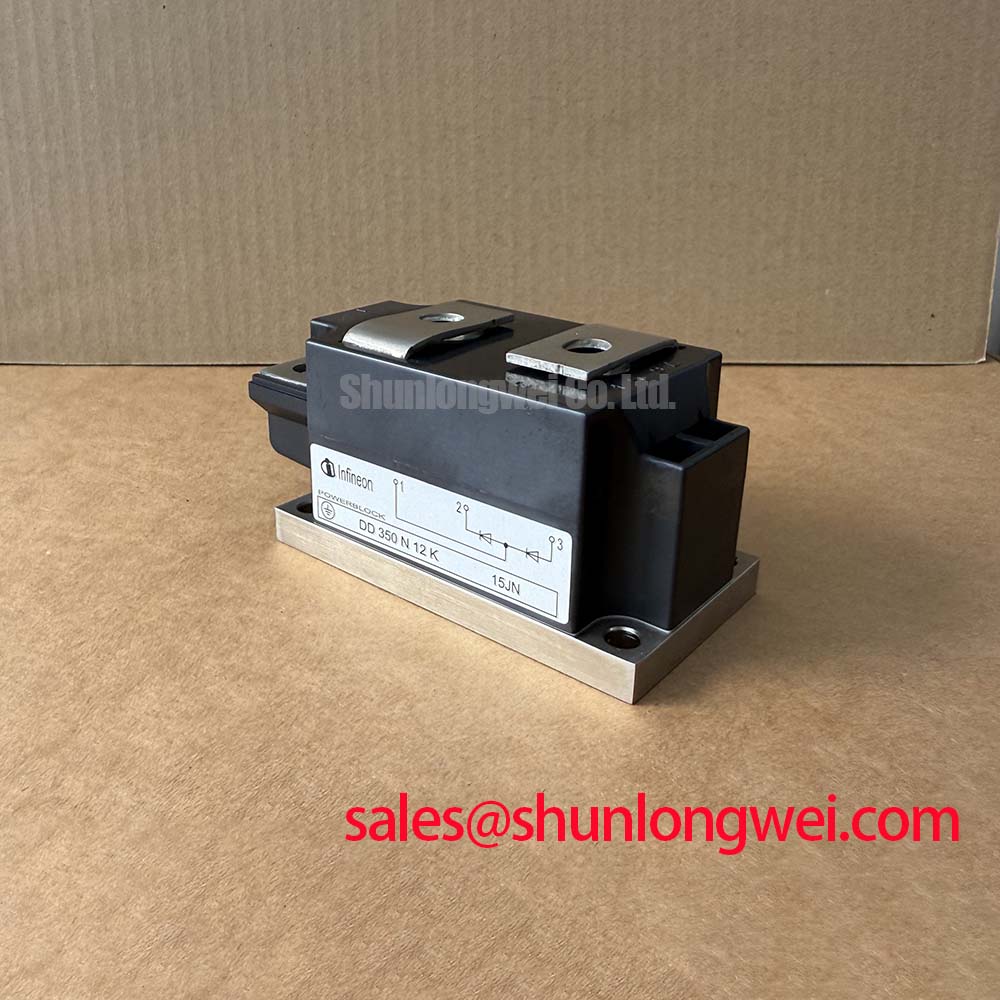
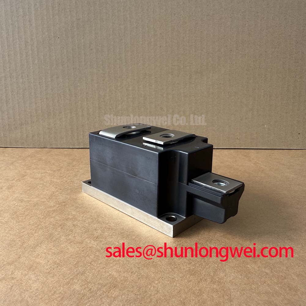
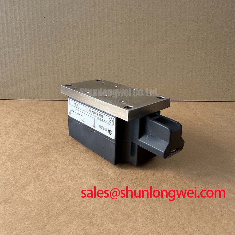
The 50 mm module package is an Official Datasheet Specification relevant to mechanical interchange assessment, but footprint size alone does not establish terminal compatibility. Before installation, confirm conductor hole positions, terminal polarity, creepage and clearance paths in the assembled product, and the clearance of covers or barriers. For a circuit exposed to high voltage, insulation spacing must be evaluated against the applicable equipment standard, contamination conditions, altitude requirements, and actual enclosure construction.
A current rating comparison can also be useful during a documented assessment. The TD210N12 is a separate device reference for engineers reviewing related 1200 V module options. Its ratings, topology, package dimensions, thermal behavior, and connection details require independent verification; no direct replacement conclusion follows from a shared voltage class.
Benchtop Waveform Tuning: Mitigating Stress via High−di/dt Commutation and Pulse−Train Timing on DD350N12K
The DD350N12K is specified here as a diode module, so it has no gate firing terminal, gate pulse rise time, holding current, or pulse train requirement to tune. Those controls belong to the thyristor, IGBT, or other actively controlled device located elsewhere in the power stage. This distinction matters during bench fault isolation: a waveform concern associated with firing pulses should be traced through the controller, isolation barrier, gate drive return path, and controlled semiconductor before drawing conclusions about the diode module.
For a thyristor switched capacitor or static var compensator assembly, timing changes can alter commutation conditions and the current waveform presented to passive rectifier elements. An Engineering Recommendation is to capture the controller command, isolated drive output, relevant power terminal voltage, and line or branch current together against a known equipment state. This establishes whether a disturbance occurs before or after the active device is commanded and avoids treating one waveform symptom as a single certain fault cause.
Industrial drive boards frequently use optocouplers or digital isolators between low voltage control logic and high energy switching sections. Their common mode transient tolerance, supply integrity, layout, and return current path should be evaluated against the original controller documentation. The DD350N12K reverse voltage and current ratings do not specify the performance of those isolation components. Designers should verify the complete drive and protection response under representative electrical noise, observing equipment safety procedures and the original test method.
Where desaturation sensing, soft turn off behavior, or short circuit protection is present, those functions concern the active switching semiconductor and driver architecture. They should remain configured according to the original equipment design. A passive diode module cannot provide gate controlled protection, and its 350 A average current rating at 100°C case temperature must not be used as a proxy for short circuit safe operating area.
DD350N12K Thermal−Electrical Optimization: Thermal Interface Material Spreading for Practical Tuning
Thermal inspection starts by removing residue from the heatsink interface, checking the mounting plane for damage, and reviewing the removed module for uneven contact patterns. The official Tvj range of −40°C to +150°C identifies the specified junction temperature boundary, while the actual junction temperature in service depends on loss conditions, heatsink performance, coolant or airflow, interface condition, and load profile. No thermal resistance value should be assumed where it is not supplied in the available product data.
As a Design Consideration, apply thermal interface material as a controlled thin, continuous layer suitable for the original mounting method. The aim is to fill microscopic interface irregularities without creating a thick insulating layer or contaminating electrical contact surfaces. Tighten mounting hardware in the documented sequence and torque specified by the equipment or module mechanical documentation. When no applicable published torque specification is available, the system integrator should obtain it from the original mechanical design rather than infer it from the package size.
Uniform mounting pressure helps preserve contact across the baseplate and heatsink, but module distortion, warped cooling plates, burrs, or trapped debris can alter the thermal path. After reassembly, compare temperature distribution and electrical behavior with a known acceptable unit where the maintenance procedure permits. Changes in case temperature may indicate interface, airflow, loading, sensing, or upstream switching differences, so the thermal result should be reviewed with the complete power path.
For broader context on cooling architecture choices, review The Advanced Thermal Management Revolution. Its discussion is useful for system level evaluation, while the DD350N12K installation must remain governed by this module’s confirmed package interface and the host equipment design. Infineon also publishes background material on automotive qualified power modules and intelligent power modules; these resources describe different product contexts and should not be interpreted as DD350N12K certifications or features.