




Content last revised on September 23, 2026
1MBI600LN-060 Thermal Electrical Optimization: Optocoupler vs Digital Coreless Transformer Practical Tuning
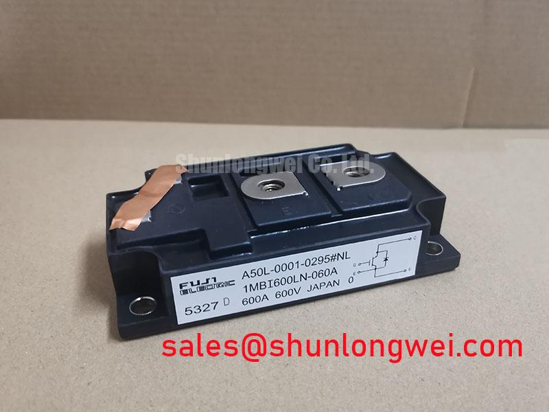
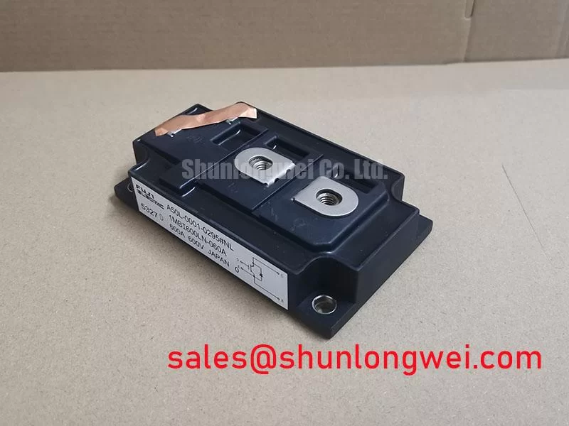
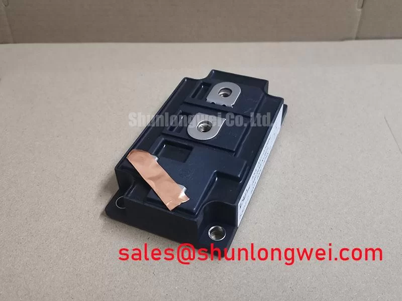
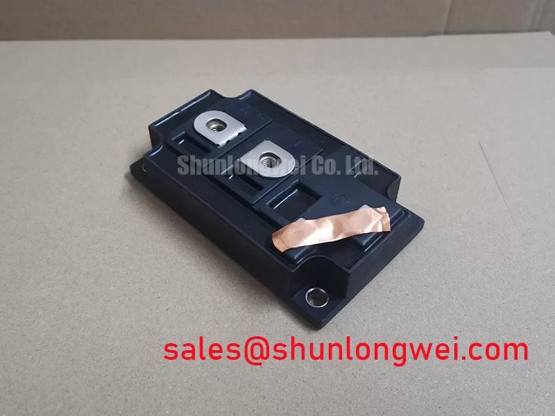
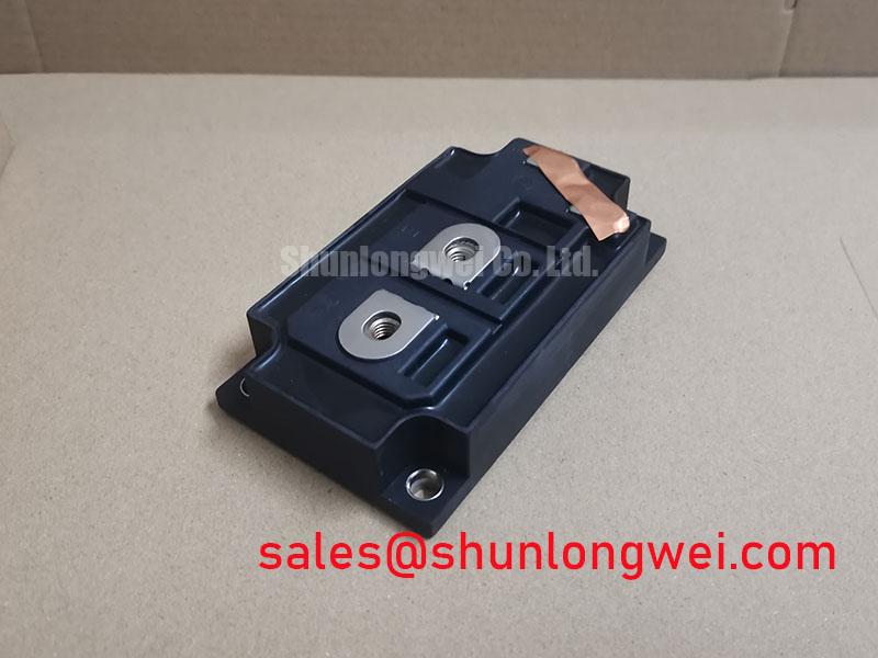
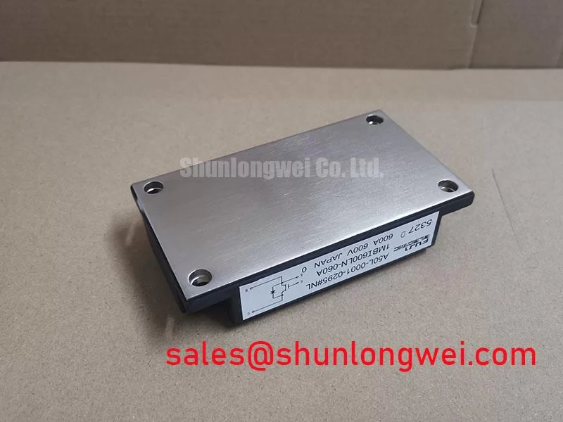
Begin commissioning by checking the nameplate against the approved bill of materials, confirming the Fuji Electric 1MBI600LN-060 is rated at 600.0 V and 600.0 A, and inspecting the module body, terminals, mounting surface, and gate wiring before energizing the converter. The official product category is IGBT Module with a Module enclosure. These values identify the component boundary; they do not by themselves establish the permissible switching frequency, short circuit duration, thermal operating point, or suitability for a complete 1500 V photovoltaic inverter.
For a utility scale central photovoltaic inverter, the first integration question is topology. A 600 V IGBT rating cannot be treated as a direct 1500 V DC link rating. The system designer should verify the number of series connected switching positions, transient voltage distribution, balancing method, insulation coordination, and measured peak VCE during switching. The final decision belongs to the converter design and its validated operating envelope, not to the module name alone.
The gate driver interface should be selected after the actual isolation barrier, control architecture, fault response, and common mode environment have been documented. An optocoupler gate driver can be evaluated where the control system requires galvanic separation and a well defined transfer path. A digital coreless transformer driver can also be considered where its isolation construction, propagation behavior, supply arrangement, and common mode transient immunity match the switching environment. The specified requirements for reinforced isolation above 5 kV or CMTI above 100 kV/µs must be verified from the selected driver documentation; they are not official ratings supplied here for the 1MBI600LN-060.
Keep the gate drive loop physically compact and route the outgoing and return paths together to reduce magnetic loop area. Separate high current commutation paths from the control isolation boundary, and avoid routing the gate signal alongside the collector switching node for long parallel distances. The exact creepage and clearance values must be established from the working voltage, pollution degree, material group, altitude, and applicable equipment standard. A general spacing number would be misleading without those conditions.
When a bootstrap arrangement is used in the driver supply, the engineering review should cover capacitor recharge time, leakage, gate charge demand, driver quiescent current, diode reverse recovery, and the minimum low side conduction interval available for recharge. High frequency charge and discharge behavior can create an undervoltage event even when the nominal auxiliary supply appears correct. Confirm the driver supply at the pins with a probe arrangement that does not include excessive probe loop inductance, then compare the measured waveform with the known good switching channel.
Negative gate bias may be considered when the measured common mode ground bounce or Miller coupling creates an unwanted turn on risk. Its value and timing are system determined and must be checked against the selected driver output capability and the module’s official gate-emitter limits in the applicable datasheet. Do not assume that a negative cutoff voltage is automatically suitable for this module without verifying the original gate drive specification.
For related topology research, the IGBT Design & Integration guide provides a broader engineering reference for gate drive, thermal management, and circuit layout. Fuji Electric also publishes information on Brake Chopper IGBT Modules and 7th Generation X Series IGBT Modules; those product families should not be assumed interchangeable with the 1MBI600LN-060 without a parameter by parameter review.
Transient Dynamics and Electrical Design: Dynamic Power Loss Dissipation and Multi R on 1MBI600LN-060
The official electrical identity of this part is straightforward: 600.0 V rated voltage, 600.0 A rated current, and a Module package. Dynamic loss analysis requires substantially more information, including switching energy under the intended current and voltage, gate resistance, junction temperature, freewheeling diode behavior, PWM conditions, commutation stray inductance, and the thermal impedance curve from the manufacturer’s technical documentation. These values should be collected before calculating a junction temperature margin.
A transient thermal model normally represents the junction to case path with several thermal resistance and capacitance sections rather than a single steady state number. In practical work, apply the measured or documented switching and conduction losses to the model, then compare the predicted case and junction temperatures with temperature measurements made under the real duty cycle. The calculation is only useful when its loss inputs reflect the actual switching waveform. Replacing them with nominal current alone can hide the effect of turn on loss, turn off loss, diode recovery, and pulse repetition.
During bench testing, place voltage and current probes so that the switching event is captured at the module terminals rather than inferred from a distant bus point. A collector voltage overshoot can be produced by commutation inductance, diode recovery, layout coupling, or an incorrectly damped snubber. The peak should be compared with the module’s official voltage boundary and the complete converter’s transient limit. Minimize parasitic loop inductance as a design consideration, then validate the result with oscilloscope measurements at the intended operating temperature and load.
The freewheeling diode’s reverse recovery behavior affects both the IGBT turn on event and the stress placed on the DC link. A sharp recovery current can increase local voltage overshoot and radiated noise, while a slower recovery characteristic can extend overlap loss. The correct interpretation requires the diode data and the actual commutation path. If the waveform shows excessive ringing, evaluate the physical loop, gate timing, snubber placement, DC link capacitor connection, and probe technique together rather than assigning the symptom to one component.
A MOV may be included in a coordinated overvoltage absorption network, but its voltage rating, energy capability, repetition duty, clamping behavior, and thermal coordination must be selected for the complete bus and fault environment. A MOV should not be treated as a substitute for low inductance layout or an appropriately designed snubber. The system engineer should verify that the MOV remains compatible with the maximum continuous operating voltage and does not introduce an unacceptable leakage or aging condition.
High frequency bootstrap operation deserves the same attention. The recharge diode must recover cleanly within the available recharge interval, and the capacitor must retain adequate driver supply voltage during the high side pulse sequence. Measure the capacitor voltage during the most demanding duty cycle, including startup, light load, maximum modulation, and fault recovery. If the measured supply droops, review the recharge path, driver consumption, switching timing, and capacitor selection using the original driver manufacturer’s limits.
For a neutral comparison point during procurement review, engineers may examine the published information for 1MBI200S-120. Its presence in a related evaluation does not establish electrical or mechanical interchangeability. Voltage class, current rating, internal circuit arrangement, terminal geometry, gate characteristics, thermal interface, and switching performance all require confirmation before any substitution decision.
Field Diagnostics and Commissioning: Thermal Feedback in 1MBI600LN-060 Topologies
Commissioning should begin with a de energized inspection and a documented cold state. Check terminal cleanliness, busbar alignment, insulation condition, torque records, heatsink flatness, thermal interface condition, and the routing symmetry of parallel gate conductors. Then measure the gate driver supply and command waveform at the module terminals. A control signal that looks correct at the driver output may be distorted by common impedance, ground bounce, probe reference error, or a damaged interconnect before it reaches the gate terminal.
Thermal feedback is useful when interpreted with the complete electrical test record. The VCE(sat) temperature behavior can contribute to a tendency toward static current balancing in appropriately paralleled devices, but dynamic sharing remains strongly influenced by gate loop impedance, driver timing, commutation inductance, physical placement, and thermal coupling. Engineers should match the gate loop geometry and use equivalent conductor paths where the topology requires parallel current paths. The balance must be verified by measured current and voltage waveforms, not inferred from static resistance checks alone.
During a loaded test, record case temperature, heatsink temperature, air path condition, switching waveform, current distribution, and the temperature rise at the main terminals. Repeat the measurement after the equipment has reached a stable operating condition. A rising terminal temperature can be associated with contact resistance, current imbalance, inadequate cooling, or an abnormal waveform, so inspect all of these possibilities. Compare the result with a known good phase or channel only after confirming that the loading and measurement locations are equivalent.
Dust accumulation on the heatsink and restricted cabinet airflow can raise case temperature without any change to the semiconductor command signal. The thermal interface material should be inspected for pump out, contamination, uneven application, or aging during scheduled maintenance. Condensation control is also important in equipment exposed to low temperature storage followed by rapid energization. Allow the enclosure and heatsink to reach a stable dry condition before applying high voltage, following the equipment manufacturer’s maintenance procedure.
Maintenance Note: Record heatsink cleanliness, terminal temperature rise, airflow condition, and thermal interface status at each planned service interval before returning the converter to operation.
For a large photovoltaic inverter, the front end may include a separate rectification stage or another complementary power stage. The 6MBI15L-060 can be reviewed as a related component reference in system topology discussions, but the circuit function, voltage class, current requirement, and mechanical interface must be checked independently. A component used in an upstream stage should not be presented as a direct replacement for the 1MBI600LN-060.
If a gate waveform is absent, first verify the driver supply, isolation channel, enable state, protection latch, gate return path, and oscilloscope reference. If the waveform is present but the collector waveform is abnormal, examine the commutation loop, freewheeling path, DC link impedance, and load condition. If thermal behavior differs between nominally similar channels, inspect current sharing, gate timing, mounting pressure, thermal interface, and sensor placement together. This approach avoids treating one field symptom as proof of a single internal failure mechanism.
1MBI600LN-060 Operational Boundaries: Evaluating Fault Clearing Dynamics and Type I or II Desaturation Limits
Short circuit protection must be designed around the selected gate driver and the documented short circuit safe operating area of the specific module. The requested Type I and Type II desaturation response below 10 µs should be treated as a system design target for evaluation, not as an official rating of the 1MBI600LN-060 based on the data supplied here. Confirm the actual detection delay, blanking behavior, comparator threshold, soft turn off profile, gate clamp action, and fault reset sequence from the driver documentation and the module’s original datasheet.
Desaturation sensing should be tested with the real collector voltage transition, diode behavior, wiring parasitics, and fault current path. A bench resistor or low energy test may not reproduce the voltage stress and current rise seen in the converter. The test plan should therefore define how the fault is initiated, where voltage is measured, how current is limited, and how the equipment is isolated after protection activation. The peak collector voltage during a protected turn off must be checked against the module’s 600.0 V official rated voltage and the validated transient margin of the complete design.
A two stage soft turn off strategy can be evaluated when a rapid gate transition would create excessive inductive overvoltage. The first stage reduces the gate drive in a controlled manner, while the second stage completes turn off after the driver has managed the initial fault current transition. The timing, gate current, clamp behavior, and fault energy are determined by the protection circuit and system inductance. They must be tuned with actual waveforms rather than copied as fixed values from another IGBT family.
Common mode noise can interfere with desaturation sensing, isolation feedback, and the fault latch. Keep the sensing return path separated from high di/dt power conductors, minimize unwanted coupling into the gate loop, and verify the protection signal with differential probing. If a fault is reported during normal switching, compare the desaturation waveform with the collector voltage, gate voltage, load current, and driver supply at the same time base. This can help distinguish switching noise, incorrect blanking, inadequate sensing layout, and a genuine overcurrent event without assigning a premature cause.
Overvoltage protection should be coordinated with the DC link capacitor network, local snubber, MOV selection, gate control, and mechanical busbar arrangement. The protection circuit can reduce fault consequences, but it cannot remove the stored energy of a high power DC link. The equipment designer must verify discharge, isolation, interlock, and restart behavior under every defined fault state.
Before releasing a repaired assembly, repeat insulation checks, gate signal checks, low energy switching checks, thermal observation, and controlled load commissioning according to the equipment procedure. Record the measured values against the approved design file and the original component documentation. The product reference remains Fuji Electric 1MBI600LN-060, rated at 600.0 V and 600.0 A in a Module package; all switching, protection, thermal, and system-level limits require verification in the intended converter.