

Content last revised on October 18, 2026
2MBI400U2B-060-50 Operational Boundaries: Evaluating PCB Gate Loop Layout Symmetry Limits
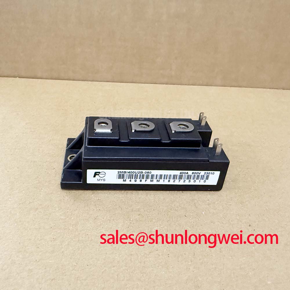
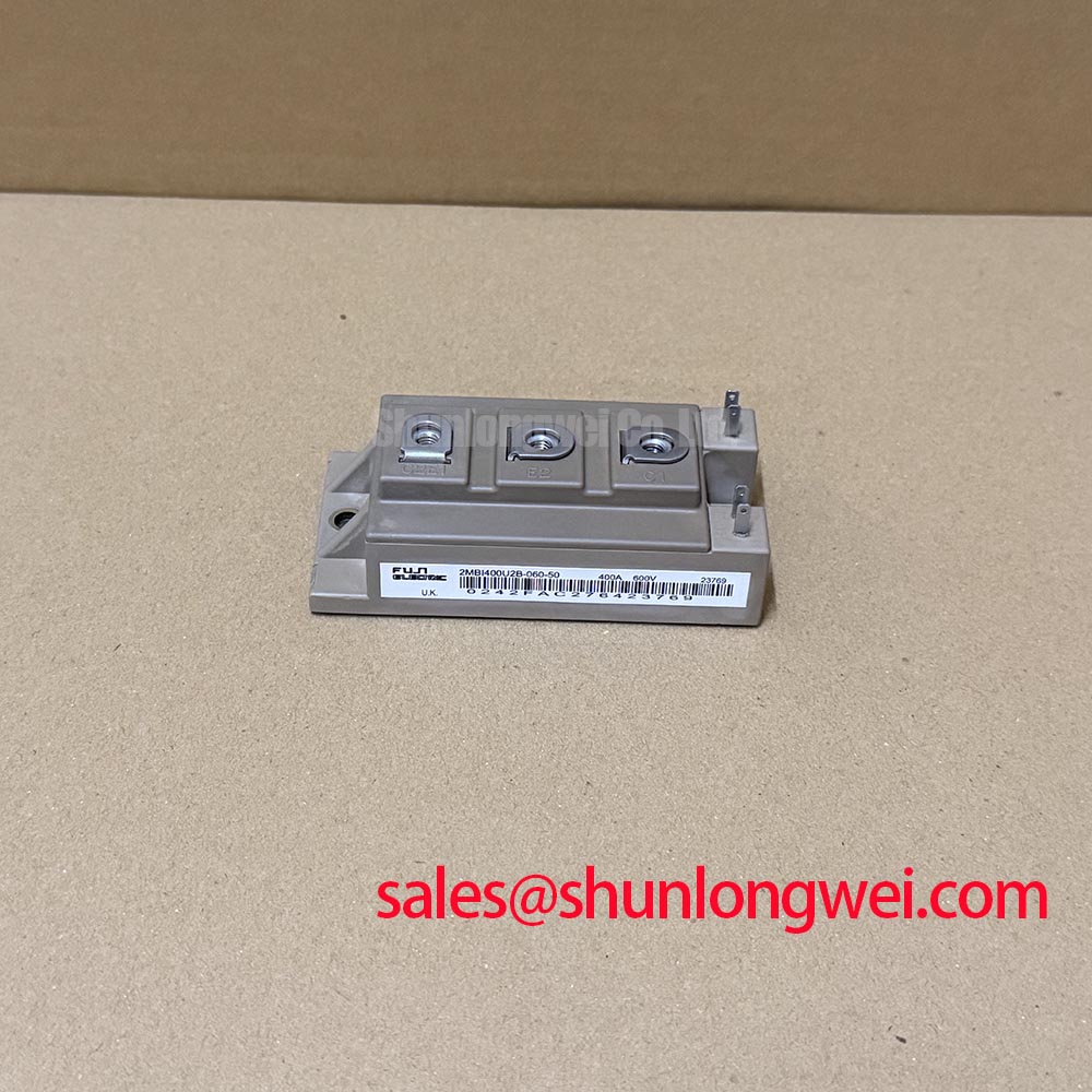
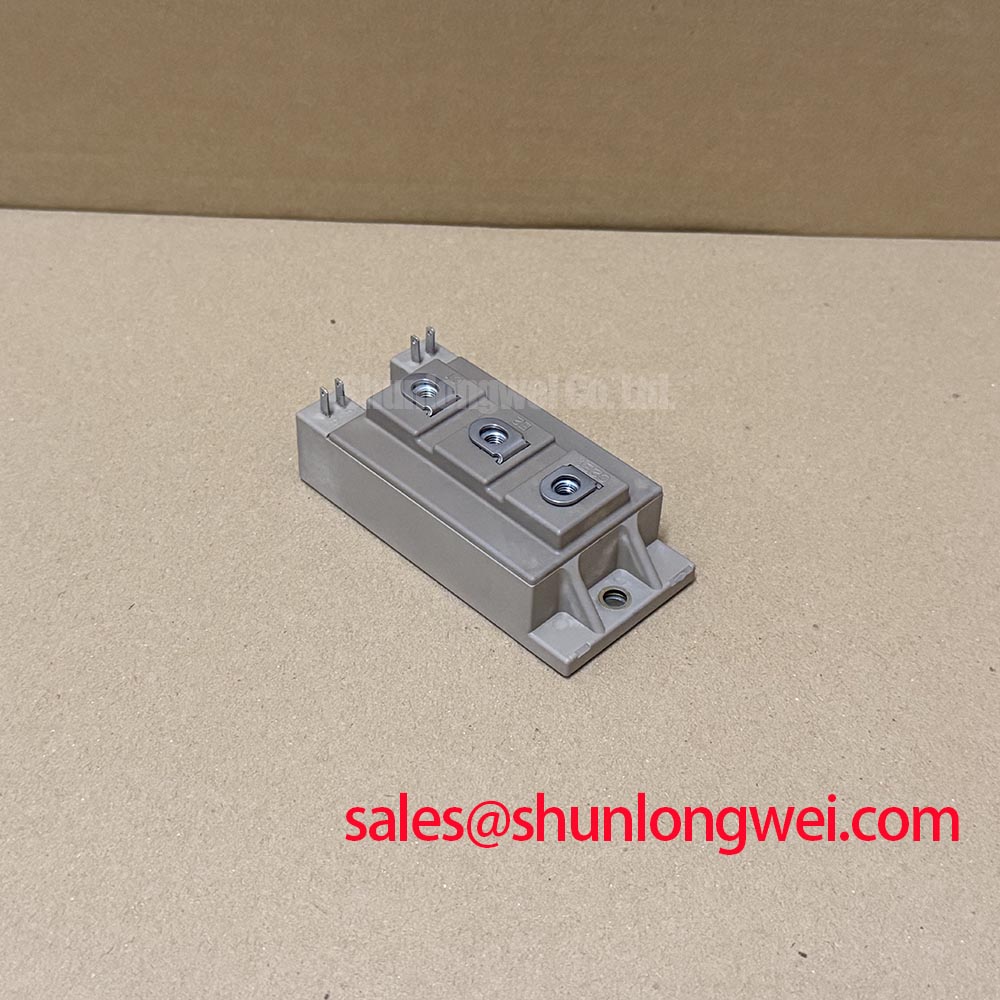
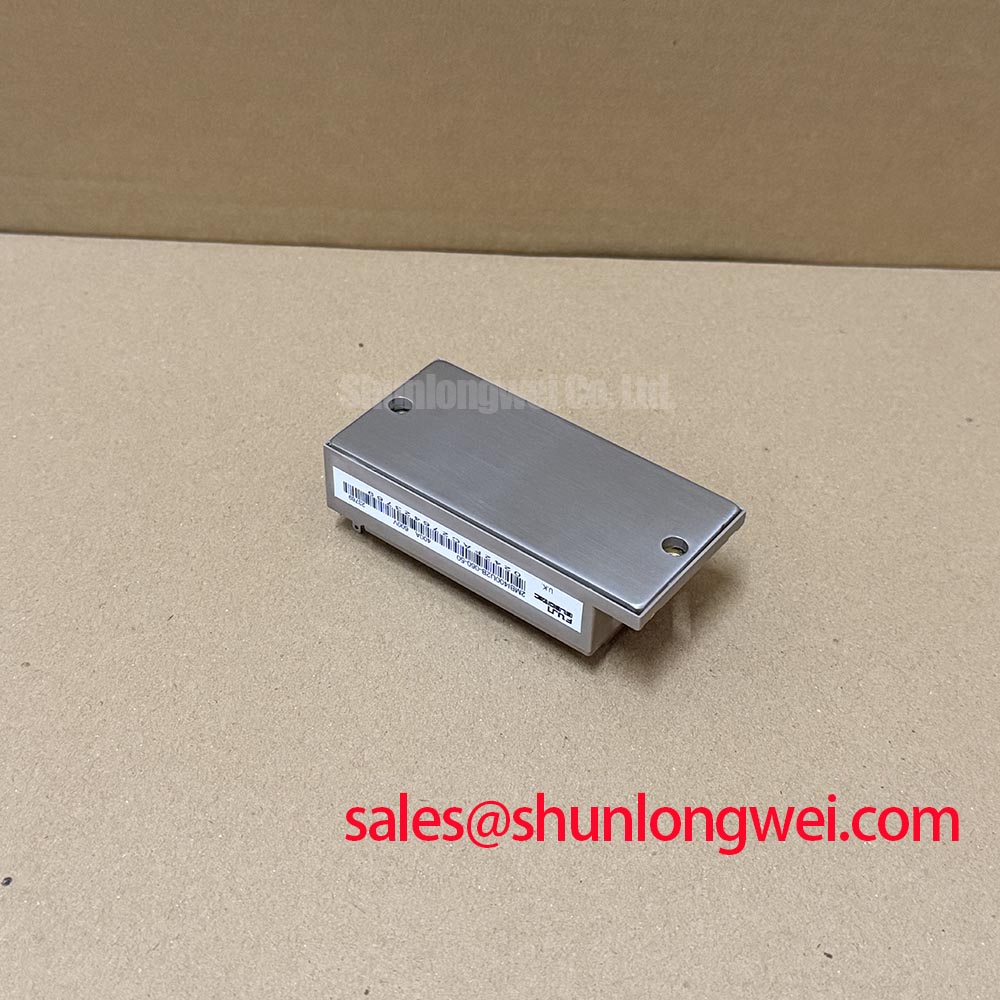
Check the nameplate and module terminals against the replacement record, then inspect the power terminals, gate wiring, and case for contamination or mechanical damage before reconnecting the converter. The 2MBI400U2B-060-50 is a Fuji Electric IGBT module specified for a 600 V collector emitter voltage and a 400 A continuous collector current at Tc = 80°C.
| Parameter | Value | Classification |
|---|---|---|
| Manufacturer | Fuji Electric | Product identification |
| Product category | IGBT module | Functional category |
| Collector emitter voltage, VCES | 600 V | Official datasheet specification |
| Continuous collector current, IC | 400 A at Tc = 80°C | Official datasheet specification |
| Collector emitter saturation voltage, VCE(sat) | 1.70 V at Tj = 25°C | Official datasheet specification |
| Junction to case thermal resistance, Rth(j-c) | 0.08°C/W for the IGBT | Official datasheet specification |
| Module housing and suffix | 2B / −50, RoHS | Official product information |
For a utility scale centralized battery energy storage PCS, the practical starting point is to compare the removed module’s gate return path with the replacement installation. Keep the gate drive route physically separate from the high current emitter and collector conductors wherever the mechanical layout allows. A gate return that shares impedance with the main emitter path can transfer switching voltage into the driver reference, so the power loop and control loop should be traced separately during inspection.
This is a Design Consideration, not an additional Fuji Electric rating. Designers should keep parallel gate paths similar in length, routing layer, connector arrangement, and return geometry when several switching positions are used. The auxiliary emitter or driver return must not be treated as an interchangeable substitute for the main high current emitter connection unless the original circuit documentation confirms that function. Confirm terminal identity from the equipment schematic and the applicable module documentation before applying a gate signal.
During a field check, isolate the DC link, discharge it according to the PCS service procedure, and inspect the gate resistor, driver supply, isolation components, and connector seating. A resistance comparison between corresponding gate paths can reveal an open resistor, damaged connector, or altered return route, but a static resistance result cannot prove switching health. If the PCS shows uneven phase current or intermittent gate faults, use an oscilloscope on a known good reference path and compare gate to emitter voltage, turn on timing, turn off timing, and the power terminal waveform under a controlled test condition.
The listed VCES rating of 600 V defines an important device boundary, but it does not define the complete transient margin of a converter. DC link voltage, stray inductance, switching speed, snubber behavior, and gate drive conditions must be evaluated together. Engineers assessing this module for a battery energy storage PCS should verify the actual peak voltage at the module terminals during switching tests rather than infer it from the nominal bus voltage alone.
Benchtop Waveform Tuning: Mitigating Hard Switching Transients via 2MBI400U2B-060-50
Bench tuning should begin with low energy and controlled pulse conditions. Confirm that the driver can maintain a stable gate reference, that the isolation barrier is operating correctly, and that the gate loop is free from unintended coupling. The published VCE(sat) value of 1.70 V at Tj = 25°C is a specified test point, not a universal operating value for every junction temperature or current condition. It should be used with the relevant output and transfer characteristics when interpreting measured waveforms.
Short circuit protection requires system level coordination. A coordinated short-circuit response may involve desaturation sensing, gate voltage monitoring, current feedback, or a combination selected by the converter designer. The suggested response time and soft turn off profile must be taken from the module application data and the protection circuit design; they should not be treated as guaranteed values for this product page. The PCS engineer should validate whether the protection circuit detects the event within the module’s documented short-circuit capability, if specified, and should confirm the resulting collector emitter overshoot during a controlled test.
A two stage soft turn off strategy can be evaluated where a rapid initial gate reduction is followed by a controlled current fall. This is an Engineering Recommendation for bench investigation, not an official parameter of the module. The correct gate resistance, clamp behavior, and timing depend on the driver output capability, gate charge, bus inductance, load current, and protection architecture. If a high side driver uses a bootstrap supply, the bootstrap capacitor selection should account for the gate charge demanded by the switching device, driver quiescent current, leakage, refresh interval, and permissible supply ripple. The system integrator must calculate the required capacitance from the selected driver and operating sequence.
When a freewheeling diode is present elsewhere in the power stage, its reverse recovery behavior can add to turn off stress and conducted or radiated EMI. The diode softness factor and recovery current should be measured or taken from the applicable diode documentation rather than assigned to the IGBT module without evidence. Gate drive tuning should therefore be checked together with diode current commutation, busbar geometry, probe placement, and common mode current paths.
Assembly Integrity & Layout Architecture: Implementing Static and Dynamic Current Distribution
The specified junction to case thermal resistance of 0.08°C/W for the IGBT connects electrical loading to the quality of the thermal interface, heatsink condition, mounting flatness, and airflow. It is an official module specification, but the assembled PCS thermal result is determined by the complete mechanical stack. Before installation, clean the mating surfaces using the equipment maintenance procedure, check for distortion or foreign material, and confirm that the cooling path is not restricted by dust accumulation.
Positive temperature behavior of VCE(sat) can support static current sharing at suitable operating conditions, but it does not remove the need for symmetrical power and gate wiring. Dynamic imbalance can develop from unequal gate loop inductance, different driver propagation paths, unequal busbar geometry, or inconsistent contact pressure. For parallel switching positions, the layout should be mirrored as far as practical and verified through current probe measurements during turn on and turn off.
Terminal inspection should include discoloration, looseness, damaged threads, and evidence of localized heating. Torque values must come from the Fuji Electric mechanical documentation or the equipment manufacturer’s service specification; a generic fastener value should not be presented as a module requirement. ⚠️ Maintenance Note: monitor contact temperature during scheduled service and recheck heatsink airflow after cleaning, because a sound electrical waveform cannot compensate for a degraded thermal path.
For a replacement assessment, the neutral comparison reference 2MBI300U4H-120-50 should be evaluated against voltage class, current conditions, package geometry, terminal arrangement, gate requirements, thermal data, and protection limits. A similar housing or current label alone does not establish interchangeability. The maintenance team should approve any substitute only after the original PCS schematic, mechanical drawing, driver settings, and measured switching behavior have been checked.
Thyristor based input or bypass stages may exist elsewhere in a PCS, but their gate trigger requirements are separate from the IGBT gate drive. IGT, VGT, pulse width, and pulse train behavior must be taken from the thyristor manufacturer’s documentation. They should not be transferred to this Fuji Electric IGBT module or used as assumed gate drive values.
Preventing Spurious Faults: DC Link Capacitance Bank Layout and Low ESL Guidelines
Inspect the DC link capacitor bank, laminated busbar, snubber connections, and module terminals as one commutation loop. During turn off, the voltage peak is influenced by DC link voltage, stray inductance, and current change rate; this relationship explains why a physically short and tightly coupled bus structure generally reduces overshoot, but it does not provide a guaranteed limit for a particular installation. The final design must be verified with suitable differential voltage probes at the module terminals.
Plan the capacitor bank connection so that the outgoing and return conductors have closely matched geometry. Avoid long branch connections from the capacitor bank to individual switching positions, and keep snubber connections short enough to be effective at the frequency range being investigated. The required capacitance, voltage rating, pulse current capability, and damping must be determined from measured ringing, switching energy, capacitor data, and the PCS operating envelope. A capacitor value selected without checking ESL and loop placement may have little effect at the relevant transient frequency.
When a suspected fault occurs, compare the DC link voltage, gate waveform, collector emitter voltage, phase current, and temperature trend with a known good operating record. An intermittent overvoltage alarm may involve probe grounding, capacitor aging, a loose laminated bus connection, gate timing mismatch, or a protection threshold interaction. Verification should proceed by controlled measurement rather than assigning a single cause from the alarm code.
Thermal test interpretation should distinguish the module’s specified junction to case value from the complete heatsink assembly. The JEDEC JESD51 thermal test method provides industry context for thermal characterization, while the actual PCS installation still requires its own interface, airflow, and temperature verification. For longer term switching evaluation, engineers may also consult the Wide Bandgap Revolution technical reference when comparing alternative power semiconductor approaches, without treating that comparison as evidence of interchangeability or a rating for this module.