


Content last revised on September 22, 2026
Benchtop Waveform Tuning: Gate Drive Loop Geometry for 2MBI400VG-60
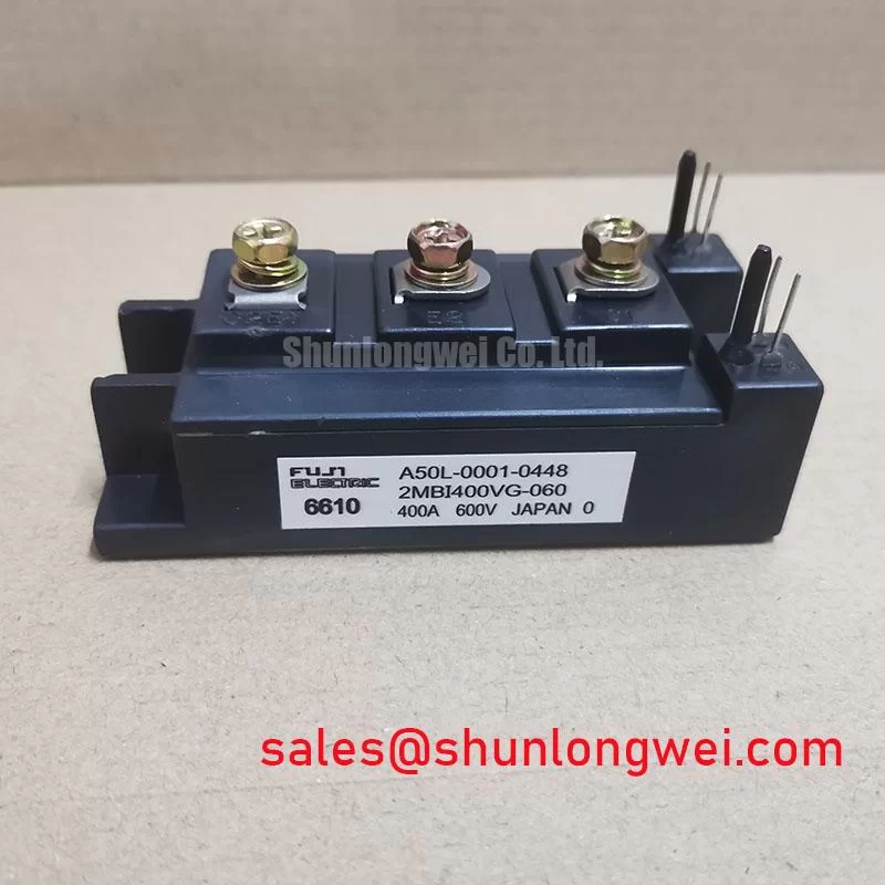
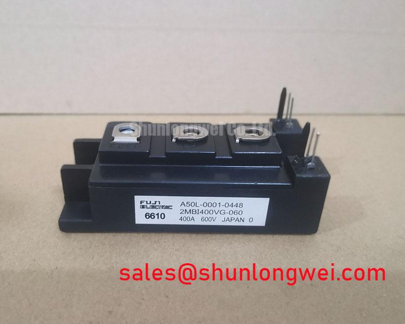
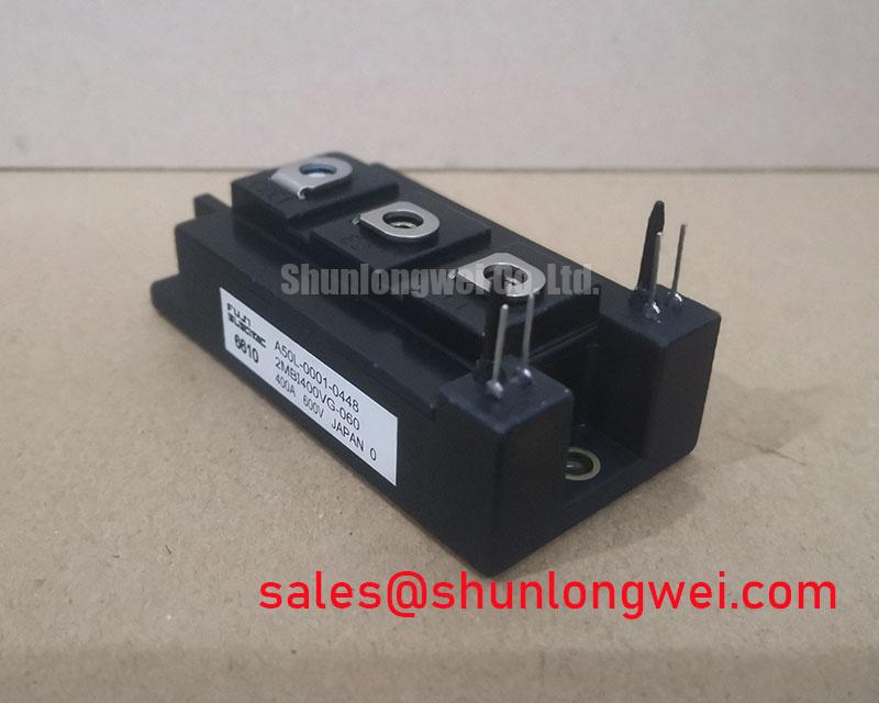
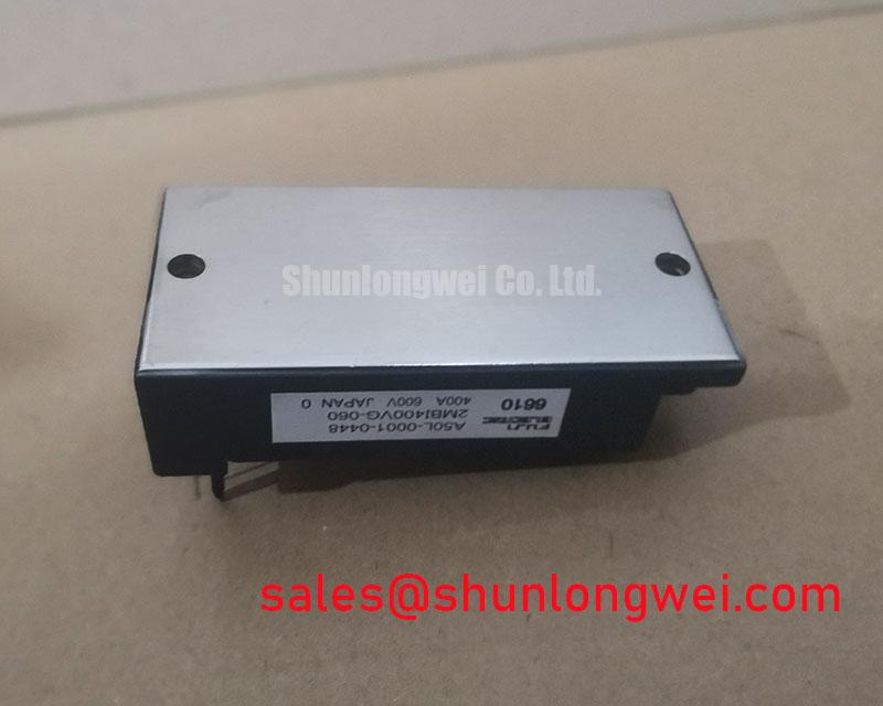
Begin the bench inspection by confirming the nameplate identity, checking the package for mechanical damage, and verifying the cold electrical condition of the installed Fuji Electric 2MBI400VG-60 against a known-good module before applying gate-drive power. The official product data supplied for this device identifies it as a 600.0 V, 400.0 A IGBT module in a module package. These ratings define the component boundary; switching frequency, gate voltage, current margin, and protection settings remain system-level decisions.
When the original circuit provides separate power-emitter and auxiliary-emitter connections, the gate-driver return should follow the auxiliary emitter reference used by the driver rather than sharing the high-current emitter path. This arrangement reduces the influence of common emitter inductance during fast collector-current transitions. Keep the gate loop compact, route the outgoing gate conductor beside its return, and avoid placing the control return through copper that also carries the main switching current.
This is a Design Consideration, not an additional Fuji Electric rating. The practical objective is to reduce parasitic loop inductance and prevent the driver from responding to voltage developed by the power-current path. If the module or the original gate-driver board does not expose an auxiliary emitter connection, the system integrator should follow the documented terminal arrangement rather than create an assumed Kelvin connection.
At the bench, inspect the gate-to-emitter waveform directly at the module terminals with a suitably rated differential probe. Compare the turn-on and turn-off edges, gate overshoot, ringing, and the collector-emitter response with the known-good signal path. A distorted gate waveform may involve driver impedance, probe placement, grounding, bus commutation, or module condition, so it should not be assigned to one cause without measurement.
Gate resistance is a tuning variable. A higher external resistance can reduce edge speed and ringing, while a lower value can increase switching speed and electrical stress. Select the initial value from the original equipment documentation or the validated gate-driver design, then evaluate the complete switching waveform under the intended DC-link and load conditions. The 2MBI400VG-60 data provided here does not specify a universal external gate resistor value.
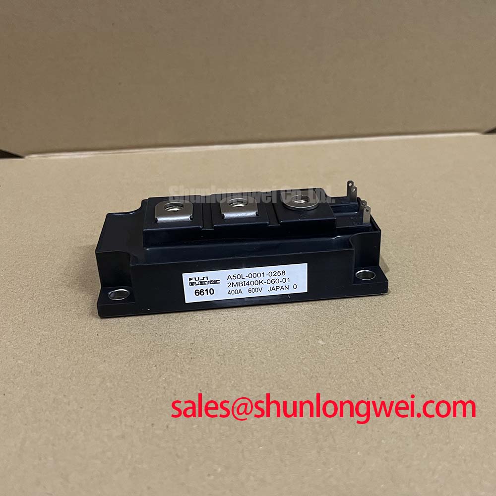
For a documented replacement review, engineers can also compare the terminal arrangement, electrical ratings, mechanical drawing, and gate-drive requirements of 2MBI400TB-060-01. That comparison should be treated as a technical cross-check rather than an automatic substitution decision.
Assembly Integrity and Layout Architecture: Common-Mode Transient Control for 2MBI400VG-60
Before connecting the module to a traction inverter or industrial converter, trace the isolation barrier from the control electronics to the high-side and low-side gate-drive stages. The required isolation withstand rating and common-mode transient immunity belong to the complete gate-driver assembly. They are not stated as standalone specifications for the 2MBI400VG-60 in the supplied product data, so the driver, power supply, PCB creepage, clearance, and insulation system must be evaluated together.
Some design references use reinforced isolation above 5 kV and common-mode transient immunity above 100 kV/µs as application targets. These figures are Design Considerations only and must not be presented as ratings of this Fuji Electric module. The responsible selection method is to verify the required withstand level, transient performance, certification basis, and pollution environment from the original converter design and the relevant component documentation.
Gate-drive sourcing and sinking capability should be checked against the selected gate charge, switching speed, driver supply behavior, and the impedance of the complete gate loop. The driver must control both positive and negative current paths without allowing the gate node to float during power-up, shutdown, fault response, or bootstrap capacitor recharge. The system designer should validate the supply sequence and driver undervoltage lockout behavior using the original schematic.
In half-bridge equipment, bootstrap charging deserves a separate inspection. Confirm that the bootstrap capacitor receives adequate recharge time and that its leakage, driver consumption, switching duty cycle, and diode recovery behavior are compatible with the operating sequence. A bootstrap network that appears correct at low frequency may show excessive droop during rapid repetitive switching. Verify the capacitor voltage at the driver pins rather than inferring it from the upstream supply.
Layout inspection should follow the actual current loops. Separate isolated control traces from collector and emitter conductors, keep the gate return paired with the gate path, and avoid routing sensitive feedback traces alongside high di/dt commutation paths. The DC-link snubber, busbar geometry, and gate-driver placement can change the measured waveform even when the module itself is unchanged.
Fuji Electric provides application information for related power semiconductor structures, including its IGBT brake chopper modules and RC-IGBT modules. These references can support topology review, but their specifications should not be transferred automatically to the 2MBI400VG-60.
2MBI400VG-60 Thermal-Electrical Optimization: Parallel Current Sharing
Parallel use requires a complete electrical and thermal review rather than a simple current multiplication. The official rating supplied for one 2MBI400VG-60 module is 400.0 A; the permissible current of a parallel assembly depends on switching conditions, cooling, busbar symmetry, protection response, and the manufacturer’s application data.
For steady-state operation, the positive temperature behavior commonly associated with IGBT collector-emitter saturation voltage can support static current balancing because a warmer device may develop a higher conduction voltage. This is a general power-electronics principle and is not a claim about an unverified curve for this specific part. Designers should confirm the relevant VCE(sat) characteristics, temperature dependence, pulse conditions, and dynamic limits from the applicable Fuji Electric datasheet.
Dynamic sharing is more sensitive to layout. Use equal electrical path lengths where practical, match the gate-loop geometry, and keep the driver reference arrangement consistent between modules. Differences in stray inductance, gate resistance, emitter routing, or local busbar inductance can cause one device to turn on or off earlier than another. Oscilloscope measurements should be taken at each module’s actual gate and emitter terminals, not only at the driver output connector.
Thermal balancing begins with the mounting surface, heatsink flatness, airflow, and interface material condition. A module with poorer thermal contact may show a different electrical waveform as its junction temperature changes. Inspect the heatsink for contamination and check whether the interface material has dried, migrated, or been disturbed during service. A thermal camera can help locate imbalance, but the measured surface temperature should be correlated with electrical current and switching data.
When this device is assessed for a high-speed rail or heavy freight locomotive traction inverter, the equipment team should verify the original topology, braking function, cooling arrangement, isolation architecture, and mechanical envelope before any parallel configuration is considered. The presence of a 600.0 V rating does not by itself establish suitability for a particular traction converter or insulation system.
For broader system-level comparison, engineers may review the related 2MBI400U4H-170 as a peripheral topology reference. It should not be treated as an automatic companion or substitute without checking the rectifier stage, bus voltage, control method, and mechanical requirements.
Transient Dynamics and Electrical Design: Baseplate Contact and Screw Installation
Prepare the heatsink before mounting by removing debris, checking the contact surface for burrs, and confirming that the module sits without rocking. The thermal interface material should form a continuous, controlled layer that fills microscopic surface irregularities without introducing excessive thickness. A commonly used installation starting range is 50 to 100 µm, but this is a general Design Consideration, not an official 2MBI400VG-60 specification; the material manufacturer and original equipment procedure take precedence.
Baseplate curvature must be assessed with the actual heatsink and mounting arrangement. Do not attempt to correct visible distortion by tightening one corner first. Uneven pressure can leave voids in the thermal interface, increase local thermal resistance, or place mechanical stress on the package. If the baseplate or heatsink does not meet the equipment drawing, correct the mechanical condition before applying electrical power.
Apply the interface material consistently across the defined contact area, using the selected material’s application method. Excess compound can migrate toward nearby surfaces, while insufficient coverage can leave dry regions. After removal of a serviced module, inspect the imprint pattern in the compound. An uneven imprint is useful evidence for reviewing flatness, clamping sequence, and contact pressure.
Fastener installation should follow the original Fuji Electric or equipment manufacturer procedure. Where no model-specific torque instruction is available, the correct torque is determined by the fastener size, thread material, washer arrangement, heatsink design, and required contact pressure; it should not be invented from the module current rating. Tighten progressively in a crosswise sequence so that the baseplate seats evenly, then verify the final torque with a calibrated tool.
⚠️ Maintenance Note: During preventive service, clean the heatsink and air path, inspect the thermal interface for aging, and trend contact-area temperature under a repeatable load before returning the converter to full duty.
Transient testing should follow mechanical assembly because thermal contact and busbar position can affect electrical behavior. After installation, verify gate waveforms, collector-emitter overshoot, diode commutation where applicable, and temperature rise under controlled conditions. The design team should compare measured peaks with the actual DC-link voltage and insulation limits rather than rely on nominal component ratings alone.
For related power-conversion design context, the engineering article The 1200 V CoolSiC™ MOSFET Advantage in Three discusses system-level switching considerations. Its technology focus differs from this Fuji Electric IGBT module, so its numerical examples and device conclusions should not be copied directly into the 2MBI400VG-60 design.