Content last revised on September 27, 2026
Field Diagnostics & Commissioning: Active Miller Clamp Implementation in 7MBR15SA140 Topologies
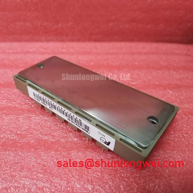
The 7MBR15SA140 product data supplied for this page identifies the device as a Fuji Electric module rated at 1400.0 V and 15.0 A. It does not confirm an internal active Miller clamp, a dedicated Kelvin emitter connection, or a specified negative gate-bias range. Active Miller clamping and negative turn-off bias are therefore external driver design considerations rather than confirmed built-in features of this product. When the module is used in a high-speed servo inverter, the gate-driver designer should verify the actual input and output arrangement from the original circuit documentation.
During a field replacement, compare the gate wiring with a known-good axis or phase. Keep the turn-on and turn-off paths physically controlled, reduce the shared impedance between power commutation and gate-return wiring, and route the driver reference according to the module’s documented terminal arrangement. The purpose is to reduce unwanted gate movement during the opposite switch transition. The correct clamp method, clamp threshold, and bias voltage remain system-determined and require oscilloscope verification under the actual DC-link and load conditions.
For a high-dynamics multi-axis CNC or robotics servo, regenerative braking can return energy to the DC bus while the axis decelerates. A braking chopper and power resistor may then absorb excess energy, but the 7MBR15SA140 should not be assigned to that role without confirming the schematic and switching duty. Check whether the module is located in the inverter bridge, braking branch, or another power-conversion stage. The resistor rating, chopper timing, DC-bus control, and thermal design belong to the complete drive system rather than to the module rating alone.
A cold resistance check is useful for screening, not for proving semiconductor health. With the equipment fully isolated and discharged, document the meter mode and test direction, then compare corresponding phase terminals with a known-good unit or an identical circuit position. A reading that differs substantially between equivalent paths may justify further testing, but it should not be treated as a standalone failure verdict. Follow with diode-mode checks where the circuit permits, then use controlled low-voltage testing and oscilloscope measurements before reconnecting the full DC bus.
High common-mode transients can disturb a gate signal when the driver reference, auxiliary supply, and power loop are poorly referenced. Designers should evaluate the physical clearance and creepage arrangement required by the complete assembly, keep sensitive driver wiring away from high-current commutation paths, and verify the real gate-to-emitter waveform at the module terminals. The Fuji Electric Power Semiconductor & IPM Modules resource is a suitable manufacturer reference point for checking the relevant product-family documentation.
Field Alert: Disconnect the DC bus and allow the equipment discharge circuit to complete before unplugging gate-drive or control connectors.
Benchtop Waveform Tuning: Mitigating Stress via Reinforced Insulation Barrier Integrity on 7MBR15SA140
Isolation performance must not be inferred from the 1400.0 V device rating. The voltage rating describes the semiconductor’s electrical blocking capability under its specified conditions; it does not confirm a reinforced insulation barrier rating, a common-mode transient immunity value, or a particular isolated-driver construction. Those values must come from the driver, interface, and module documentation used in the actual assembly.
On the bench, inspect the barrier between the control side and the power side as a complete system. Verify the creepage and clearance path on the printed circuit board, the isolation components used by the gate driver, the shield or reference strategy, and the way measurement probes are connected. A differential probe with suitable common-mode capability is preferable for observing gate-emitter voltage during switching. A conventional grounded oscilloscope lead can create an unintended current path and produce misleading waveforms or equipment damage.
Desaturation protection is a system-level function. The supplied product data does not establish a specific desaturation blanking interval, short-circuit response time, or two-stage soft turn-off behavior for the 7MBR15SA140. If the drive uses desaturation sensing, the service engineer should trace the detector connection, confirm the sense reference, inspect the blanking network, and verify the protection sequence with a controlled low-energy test. The final response time must be selected against the actual short-circuit withstand data and switching conditions in the applicable manufacturer documentation.
When the waveform shows an unexpected gate pulse, check the timing relationship between the command signal, isolated driver output, gate-emitter voltage, collector-emitter voltage, and protection feedback. A narrow disturbance can result from layout coupling, driver saturation, measurement-loop pickup, supply instability, or an incorrect reference connection. Do not assign a single cause from the waveform shape alone. Compare the suspect axis with an operating axis under the same probing method and load state.
For servo drives with frequent acceleration and deceleration, the bench test should include the actual regeneration sequence rather than only a static output test. Confirm that the DC-link controller, braking path, and inverter switching sequence remain coordinated. A phase-leg waveform that appears acceptable during motoring may show different overshoot or gate interaction during regenerative operation. Minimize parasitic commutation-loop inductance as a design consideration, then verify peak voltage against the system DC-link boundary during switching tests.
The 2MBI200PB-140 may be reviewed as a related power-stage reference when examining the upstream rectifier or complementary section of a drive topology. It should not be treated as an automatic substitute for the 7MBR15SA140. Pin arrangement, electrical role, control method, cooling interface, and switching duty must be checked from the original equipment documentation.
7MBR15SA140 Thermal-Electrical Optimization: SCSOA Overcurrent Protection and Practical Tuning
The official parameters supplied for this product establish 1400.0 V rated voltage and 15.0 A rated current. They do not establish a short-circuit safe operating area, a specified short-circuit duration, a desaturation response interval, or a guaranteed two-stage soft turn-off sequence. These limits are essential when the module is placed in a servo inverter or braking converter, so the repair decision should remain conditional until the relevant Fuji Electric data and the original drive protection design have been checked.
In practical troubleshooting, begin with the event record from the drive controller. Determine whether the trip occurred during startup, acceleration, deceleration, current reversal, or a DC-bus disturbance. Inspect the gate-driver supply, fault latch, current sensor, desaturation path if present, and the power-loop connections. A damaged module may be a result of a protection event rather than its initial cause. Replacing it without checking the gate command and overcurrent chain can expose the replacement to the same abnormal condition.
Two-stage soft turn-off is an engineering recommendation that may be considered where the system documentation supports it. The first response limits the rate of current interruption, while a later controlled turn-off completes isolation of the faulted switch. The actual timing, gate resistance, clamp behavior, and fault-energy limit must be determined by the drive designer and validated with a controlled test. Do not copy timing values from another module family without checking its gate charge, short-circuit capability, driver interface, and switching environment.
Thermal inspection should cover the module base, heatsink interface, fasteners, airflow, fan control, and temperature-sensor location. Uneven contact or a disturbed thermal interface can increase junction temperature even when the electrical waveform appears normal. Check for discoloration, loosened hardware, contamination, and signs of localized heating around the power terminals. The package designation is confirmed as Module, but physical dimensions, mounting-hole spacing, terminal torque, and thermal resistance are not specified in the supplied product data and must be taken from the correct mechanical drawing.
When the drive includes a high-power braking resistor, inspect the resistor contactor or chopper path, overtemperature switch, bus-voltage feedback, and discharge circuit. Excessive regenerative energy can stress the entire DC-link assembly. The 7MBR15SA140 rating should be assessed together with the switching frequency, duty cycle, load profile, cooling capacity, and protective shutdown sequence. These are system conditions, not independent guarantees created by the module’s voltage and current ratings.
For broader switching-device context, engineers can consult The 1200 V CoolSiC™ MOSFET Advantage in Three. That technical discussion may help with topology-level comparisons, but it does not establish interchangeability or equivalent behavior between a silicon power module and a SiC MOSFET solution.
Field Diagnostics & Commissioning: Derating Guidelines and Mismatched Parameters in 7MBR15SA140 Topologies
Parallel operation requires more than matching the printed voltage and current ratings. A positive temperature coefficient of on-state voltage can support static current sharing in some operating regions, but the behavior of a complete parallel arrangement depends on device matching, thermal coupling, gate-loop impedance, emitter-return layout, commutation inductance, and driver timing. The supplied data does not confirm a particular current-sharing capability for the 7MBR15SA140, so parallel use requires validation under the intended load profile.
When engineers evaluate multiple modules in a CNC or robotics servo, use symmetrical power paths and equivalent gate-drive routing as a design consideration. Compare gate-emitter waveforms at each device rather than measuring only the driver output. Check turn-on delay, turn-off delay, collector-emitter overshoot, current-sensor response, and heatsink temperature distribution. Any imbalance should be investigated across the electrical, mechanical, and control paths before changing gate resistance or protection thresholds.
Dead time is also system-determined. Excessively short dead time can increase the risk of cross-conduction, while excessive dead time can increase diode conduction and switching loss. The correct setting depends on the measured propagation delay, temperature, driver behavior, load current, and commutation path. Verify both directions of current flow, especially during regenerative braking, because the active devices and freewheel paths may not experience identical conditions.
Phase-controlled rectifier sections can introduce line-current distortion and DC-bus ripple that affect the inverter stage. If the 7MBR15SA140 is used downstream of such a converter, review the rectifier firing angle, DC-link filtering, line impedance, and harmonic-mitigation method at the system level. The module’s 1400.0 V voltage rating should not be used as a substitute for measuring transient bus peaks. Confirm the voltage waveform at the actual module terminals during the most demanding acceleration and braking cycles.
For procurement and replacement screening, record the original manufacturer, complete part number, package style, terminal layout, rating class, and equipment position. The 6MBI100S-140 can be considered a related reference during a specification review, but the engineer must verify pin compatibility, electrical ratings, gate-drive requirements, thermal behavior, and protection coordination before considering any alternative in the equipment.
The manufacturer reference site at Fuji Electric Global Power Semiconductor Technologies should be checked alongside the original drive manual and technical drawings. Confirm the required supply voltage, gate polarity, protection interface, mounting details, and cooling method from those documents rather than assuming compatibility from package appearance or nominal rating alone.