Content last revised on September 10, 2026
7MBR25SA140 Technical Identity and Official Ratings
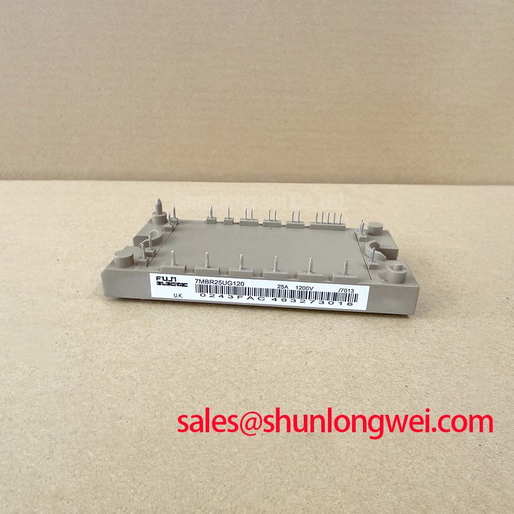
After isolating the DC link and allowing the manufacturer-specified discharge period, begin field inspection by checking the module’s part marking, housing condition, terminal alignment, and cold-state resistance against a known-good reference before reconnecting the inverter. The 7MBR25SA140 is a Fuji Electric PIM power module evaluated for industrial inverter, motor-drive, CNC servo, and robotics servo applications where voltage margin, thermal monitoring, and compact power-stage integration are important.
The available official production data identifies the module with a 1400 V collector-emitter voltage rating, a 25 A collector-current rating, and a typical 2.30 V collector-emitter saturation voltage at the stated test condition of Tj = 25°C. Its listed maximum junction operating temperature is 150°C. An integrated NTC thermistor provides a temperature-sensing interface for the host controller or protection circuit.
| Parameter | Official specification | Engineering relevance |
|---|---|---|
| Collector-emitter voltage, VCES | 1400 V | High-voltage switching boundary for system verification |
| Collector current, IC | 25 A | Current-rating reference for the inverter power stage |
| Collector-emitter saturation voltage, VCE(sat) | 2.30 V typical | Conduction-loss input for thermal evaluation |
| Maximum junction temperature, Tj | 150°C | Upper junction-temperature boundary listed for the device |
| Thermal monitoring | Integrated NTC | Supports external temperature feedback and shutdown logic |
These values are official specification data supplied for this product page, not a complete application guarantee. The system designer must confirm switching frequency, DC-link voltage, overload profile, cooling method, gate-drive conditions, insulation coordination, and the complete terminal assignment from the original Fuji Electric documentation before approving a replacement.
For a same-voltage-class comparison within an industrial power-module search, engineers can review 6MBI100S-140 as a separate reference product. It should not be treated as an automatic substitute because electrical topology, mechanical dimensions, terminal layout, gate characteristics, and protection behavior must match the original assembly.
Field Diagnostics & Commissioning: Suppressing Cres-Induced Gate Voltage Spikes in 7MBR25SA140 Topologies
Inspect for cracked resin, discolored terminals, loose mounting hardware, contamination, and signs of localized heating. A cold resistance comparison between corresponding terminals can help identify an obvious short or open condition, but it cannot validate dynamic switching performance.
Parasitic capacitance and high common-mode voltage transitions can couple energy into a gate circuit and create an unwanted gate-voltage excursion. This is a Design Consideration rather than a guaranteed failure mechanism for every installation. The practical response is to keep the gate-drive return path controlled, minimize the shared impedance between power and control returns, and route high-current commutation paths away from sensitive gate wiring. The final layout must be checked with an appropriately rated differential probe during turn-on and turn-off testing.
Low-impedance gate control, a properly selected turn-off network, and an active Miller-clamp function may be considered when the host driver supports them. A negative gate bias may also be evaluated by the system designer, but the appropriate value is system-determined and must remain within the Fuji Electric gate-emitter limits. Do not assume that a generic negative-bias setting is suitable for this module without confirming the gate-drive specification.
The same review should include the isolated driver or optocoupler. Common-mode transient immunity, propagation delay matching, isolation capacitance, and driver supply decoupling all affect the real gate waveform. A digital isolator or optocoupler with a suitable CMTI rating can reduce false triggering risk, but the complete board layout and grounding arrangement still require oscilloscope verification. The practical relationships between gate drive, thermal management, and switching topology are discussed in IGBT Design & Integration.
Benchtop Waveform Tuning: Mitigating Stress via Symmetrical Busbar Geometry for High-Current Operation
Before energizing a replacement module, verify the terminal identity against the original circuit drawing rather than relying only on physical position. Confirm the collector, emitter, gate, auxiliary return, thermistor, and any unused terminals from the product documentation. Check creepage and clearance around the power connections, especially where the module is installed close to a grounded chassis, shield, heat sink, or adjacent phase leg.
Symmetrical busbar geometry is a Design Consideration for reducing unequal stray inductance between parallel or neighboring current paths. Keep the commutation loop compact, avoid unnecessary bends, and use matched physical routing for gate connections where the circuit contains multiple switching paths. The system engineer should verify overshoot, ringing, current balance, and gate-emitter voltage with probes positioned to avoid adding a long measurement loop.
The listed typical VCE(sat) value of 2.30 V at Tj = 25°C is useful when estimating conduction loss, while the positive temperature behavior commonly considered in parallel IGBT designs can assist static current sharing. This does not remove the need to check dynamic sharing, thermal gradients, driver mismatch, and busbar impedance. A module rated at 25 A should not be treated as a universal continuous-current promise for every cooling arrangement or duty cycle.
When a MOV is used as part of the inverter protection network, its clamping behavior, energy rating, leakage current, and placement should be coordinated with the DC-link voltage and switching transient. A MOV is not a substitute for controlling stray inductance or validating the module’s peak VCE waveform. In battery-fed bidirectional DC-DC equipment, repeated charge and discharge cycles can produce thermal cycling; the integrator should correlate the NTC reading with the heat-sink temperature and actual switching waveform before establishing a service limit.
For high-current inverter routing, heavy-copper PCB construction may be evaluated where busbar integration is impractical. General background on heavy-copper conductors is available through Heavy Copper PCB. The board material and copper thickness remain system choices governed by current, temperature rise, creepage, mechanical support, and production capability.
⚠️ Field Alert: Tighten the mounting hardware only according to the original mechanical specification, apply thermal interface material evenly, and never insert or remove power-module connections while the DC link or gate-driver supply remains energized.
7MBR25SA140 Circuit Protection & Reliability: Evaluating Thermal Capacitance and Heat-Sink Response
The integrated NTC can support a controller’s over-temperature warning, current reduction, or shutdown strategy, but the NTC signal must be interpreted together with the heat-sink temperature, airflow, switching loss, and load profile. A stable measured temperature at one location does not prove that the semiconductor junction has reached the same condition. Use the NTC as part of a validated protection chain rather than as a standalone proof of safe operation.
For pulsed overloads, the thermal path should be modeled with the manufacturer’s available transient thermal impedance information. A multi-stage RC thermal network is an Engineering Calculation method that represents junction-to-case and case-to-heat-sink response over time. The resulting peak junction estimate must be checked against the official 150°C maximum junction-temperature rating, while the case temperature, interface condition, airflow, and overload repetition are measured on the actual assembly.
If a servo drive trips intermittently, record the NTC signal, DC-link voltage, phase current, switching command, and heat-sink temperature together. This helps distinguish thermal accumulation from gate-drive disturbance, current-sensor error, bus overvoltage, or mechanical cooling problems without assigning a single cause prematurely. Inspect the MOV network for thermal discoloration and leakage-related symptoms, and verify that its clamping level does not conflict with the module’s 1400 V VCES boundary during switching events.
In a bidirectional battery converter, charge and discharge operation can move heat through the same power path in alternating directions. The designer should evaluate thermal cycling, transient overload, regenerative braking, and cooling recovery under the real operating sequence. No field lifetime or failure-rate figure is assigned here because such results require a defined test bench, mission profile, and authoritative source.
Benchtop Waveform Tuning: Verifying Kelvin Emitter and Gate-Return Behavior
Do not assume a separate Kelvin-emitter connection, auxiliary emitter terminal, or equivalent low-inductance control return unless it is confirmed in the Fuji Electric terminal drawing for the exact module variant. If the original topology provides a dedicated control return, route it directly to the driver reference and keep it separate from the high-current emitter path until the intended joining point. This reduces mutual coupling that can distort the measured gate-emitter waveform.
During commissioning, measure the gate-emitter voltage at the module terminals, not only at the driver output. Compare turn-on and turn-off waveforms for ringing, delayed transitions, abnormal plateau behavior, and differences between phase legs. If the signal changes significantly when the probe location moves, the measurement loop or common impedance may be influencing the result. Recheck the driver isolation barrier, CMTI behavior, decoupling placement, and return-current path before changing gate-drive settings.
The 2MBI200PB-140 may be reviewed as a separate device within related rectifier or complementary power-stage research, but its presence in the same system does not establish pin compatibility with the 7MBR25SA140. Final approval should be based on the original schematic, mechanical fit, verified terminal mapping, thermal test data, and switching waveforms under the equipment’s actual load.