Content last revised on September 10, 2026
Preventing Spurious Faults: Overvoltage Trip Prevention via Fast Switching Guidelines for 7MBR50NH060
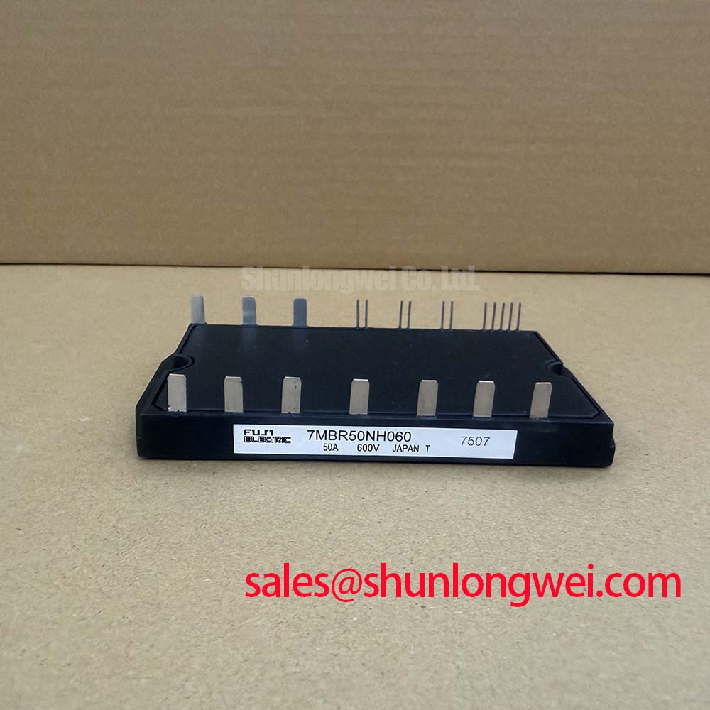
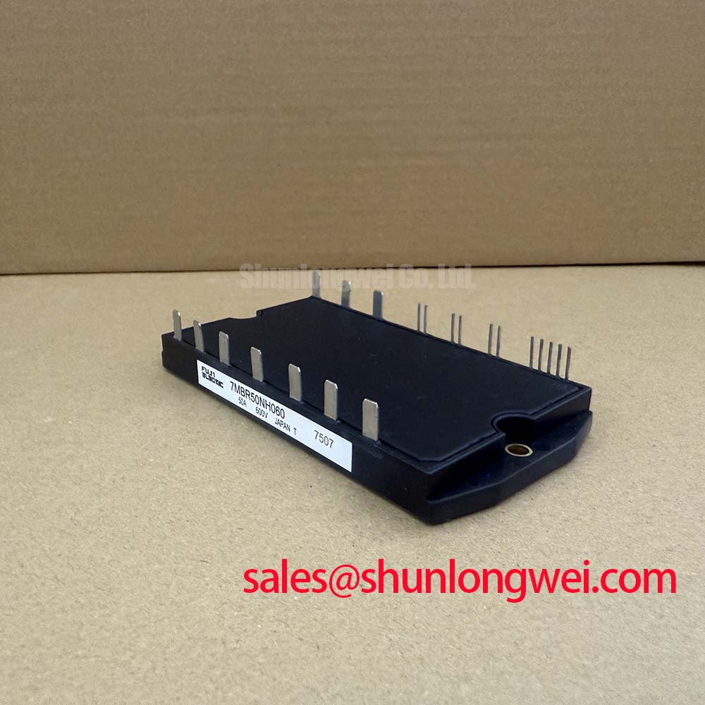
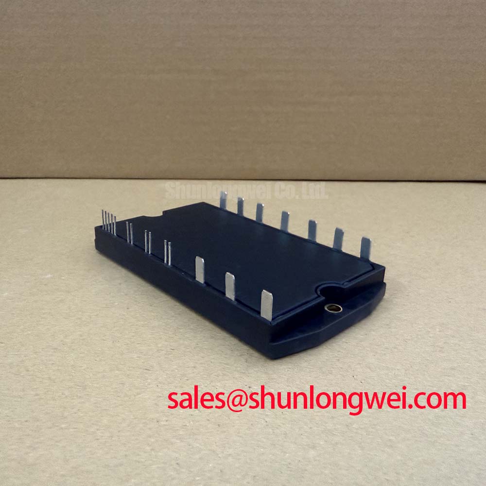
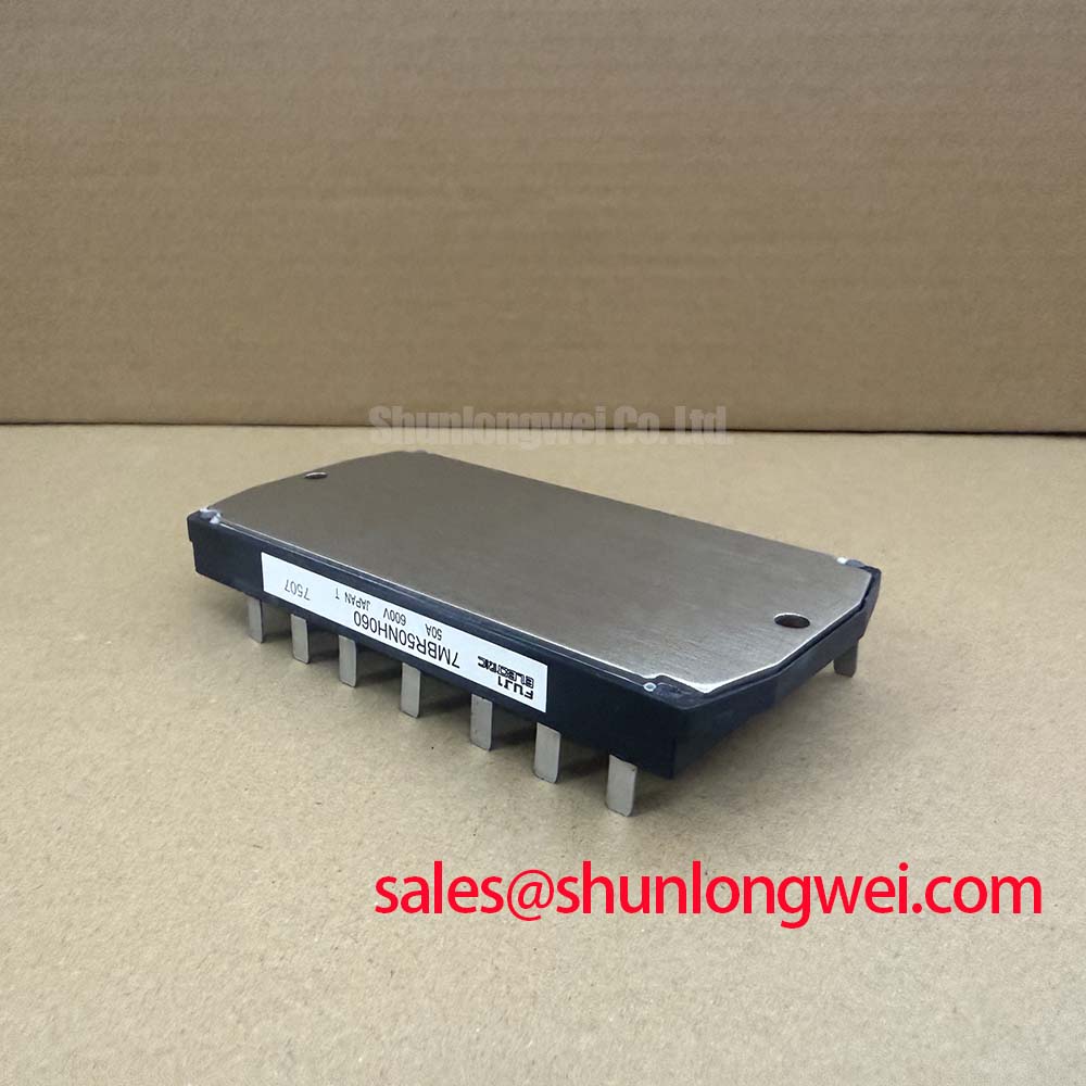
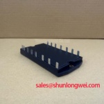
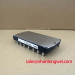
Before reconnecting a removed drive assembly, verify the nameplate electrical boundaries against the cabinet DC link and braking circuit: the 7MBR50NH060 inverter stage is rated at 600 V VCES, its rectifier stage at 800 V VRRM, and its brake chopper at 50 A IC, all Official Datasheet Specifications. This check matters when a servo drive has reported a DC bus overvoltage trip during rapid deceleration, because the braking path and the inverter path operate under different stated voltage ratings.
During motor deceleration, mechanical energy returns through the drive into the DC link. The brake chopper function is used with an external ballast resistor so that excess DC link energy can be dissipated rather than raising the bus voltage until a protection threshold is reached. The required resistor value, pulse capability, energy rating, and cooling arrangement are system determined because they depend on motor inertia, operating cycle, deceleration profile, DC link capacitance, and control strategy. An Engineering Recommendation is to inspect the existing resistor assembly for open connections, heat discoloration, loose terminals, and failed thermal protection before attributing repeated overvoltage events to the power module.
When evaluating a high dynamics multi axis CNC or robotics servo drive, engineers should capture the DC link voltage during the actual deceleration event rather than relying only on a static meter reading. Compare the measured waveform with the drive controller command, braking resistor connection, and chopper gate command where safe access is available. A rising DC link with no valid chopper activity can indicate a control, wiring, sensing, or gate drive issue. Chopper activity without adequate bus control can indicate that the resistor network or its thermal path requires further assessment. These observations are diagnostic evidence, not a single cause determination.
Layout around the braking loop remains a Design Consideration. Keep the high current path between the DC link, brake chopper connection, and ballast resistor direct and mechanically secure. Unnecessary loop area can increase inductive voltage excursion when current changes rapidly. Clearance and creepage requirements must follow the complete equipment insulation design, local standards, contamination conditions, and the physical PCB or busbar construction rather than a generic module page.
For part number comparison during a repair assessment, the 7MBR50LC060 can be reviewed alongside this unit. Engineers should confirm circuit function, terminal assignment, mechanical fit, gate drive behavior, thermal interface arrangement, and all ratings against the original equipment documentation before treating any alternative part number as interchangeable.
💡 Pro Tip: Use a compact, symmetrical busbar path around the DC link and validate turn off voltage margin with double pulse or equivalent switching tests on the completed assembly.
Field Diagnostics & Commissioning: Thermal Interface Material Thickness Uniformity in 7MBR50NH060 Topologies
The thermal installation begins with the mounting faces powered down, isolated, and cleaned of hardened compound or foreign particles. The 7MBR50NH060 has an Official Datasheet Specification isolation voltage of 2500 V AC for 1 minute; this is an electrical rating and should not be interpreted as a substitute for checking the complete drive’s insulation system, mounting hardware, heatsink condition, enclosure, and service procedures.
Thermal interface material should form a continuous, controlled layer between the module baseplate and the heatsink. A practical Design Consideration is a thin application in the general range of 50 to 100 µm where the selected material and mounting design support it. The objective is contact conformity rather than a visually thick coating. Excess material can increase thermal resistance, while insufficient coverage or trapped debris can leave local voids. Baseplate flatness, heatsink finish, and any curvature influence the result, so the contact pattern should be assessed after a controlled trial assembly when service practice permits.
Tighten mounting screws in a gradual cross pattern so clamping force is distributed across the baseplate. The final tightening procedure, tool setting, screw grade, washer arrangement, and torque must follow the equipment manufacturer’s mechanical documentation. Avoid assuming a universal torque because the correct value depends on the mounting hardware and heatsink design. After commissioning, compare temperature response and current loading with a known stable drive where possible. A localized thermal anomaly may relate to interface contact, airflow, sensor placement, switching conditions, or load imbalance and deserves measurement before a component level conclusion is made.
Freewheeling diode commutation also deserves attention when investigating radiated noise or unexplained protection events. Reverse recovery behavior interacts with bus inductance, gate drive timing, current level, temperature, and the external snubber network. An Engineering Recommendation is to inspect the original snubber capacitors, resistor networks, and their physical connections before changing gate drive components. A degraded snubber or long return path can alter ringing substantially even where the power module itself passes basic static checks.
Oscilloscope measurements should use probing methods suitable for high voltage switching nodes and the instrument’s stated safety limits. Observe the collector emitter waveform, gate emitter waveform, and DC link behavior in relation to the same switching event. The aim is to identify repeatable correlation between ringing, overshoot, thermal loading, and fault timing. No field lifetime or failure rate is implied by this procedure. For context, MTBF and reliability engineering describe population based statistical concepts; they do not establish a service life prediction for an individual installed module.
Field Diagnostics & Commissioning: DC Link Capacitance Bank Layout and Low Inductance in 7MBR50NH060 Topologies
Inspect the DC link capacitor bank at the same time as the power module. Check capacitor terminals, laminated busbar contact surfaces, fasteners, solder joints where applicable, and the physical distance between the capacitor bank and the inverter connection. In a switching loop, peak collector emitter voltage is influenced by the DC link voltage plus the inductive term created when stray inductance is multiplied by the rate of current change. This Engineering Calculation principle explains why a drive can show switching overshoot even though its steady DC bus is within the nominal operating expectation.
The 600 V VCES inverter rating is an Official Datasheet Specification, so measured transient peaks should be assessed against that stated boundary under the actual operating conditions. Designers should minimize parasitic loop inductance to suppress turn off overshoot, then verify peak margins against the DC link voltage during controlled switching tests. The acceptable inductance target, switching rate, snubber configuration, and capacitor selection belong to the full drive design and should be established by the system engineer rather than assigned as fixed values for this module.
A planar, closely coupled positive and negative bus arrangement is often evaluated because it reduces enclosed loop area. Capacitors intended to support fast switching current should be connected with short, broad paths to the relevant power terminals, while lower frequency bulk energy storage can be assessed separately. Do not use the module’s 800 V VRRM rectifier stage rating to justify higher inverter DC link operation; each functional block must be evaluated against its own Official Datasheet Specification and the complete topology.
In field repair, an intermittent overvoltage trip may arise from several interacting conditions, including capacitor degradation, loose busbar joints, altered wiring geometry, an ineffective snubber, gate drive changes, or an abnormal load event. Look for waveform differences between a known good axis and the affected axis when the machine architecture permits comparison. Verify capacitor condition using methods appropriate to the equipment and component documentation. Static capacitance alone may not reveal all high frequency or connection related concerns.
At demanding operating boundaries, system engineers sometimes compare different power semiconductor approaches as part of a broader design review. The technical discussion in The 1200 V CoolSiC™ MOSFET Advantage in Three provides a reference point for examining switching behavior in three phase power conversion. It should be used for engineering context rather than as a claim that the 7MBR50NH060 shares the characteristics of a different device technology.
Field Diagnostics & Commissioning: Active Miller Clamp Implementation in 7MBR50NH060 Topologies
Gate drive behavior should be checked dynamically after confirming the DC link and thermal interface condition. During a rapid voltage transition, capacitive coupling through the switching device can raise the gate potential of the opposite switch. If that induced voltage approaches the effective turn on condition, unwanted conduction can occur. The risk is affected by driver output impedance, common emitter inductance, gate return routing, switching speed, load current, and the actual module and PCB arrangement.
An active Miller clamp is a Design Consideration for gate driver circuits that provide this function. It creates a low impedance gate to emitter path during the off state, helping resist induced gate movement. Whether the existing driver supports an active clamp, the correct connection point, and its turn on and turn off timing must be verified from the original gate driver documentation and circuit schematic. Do not add a clamp circuit or alter gate bias solely from a generic recommendation, because the result must be evaluated with the installed driver and protection architecture.
Negative gate bias is also a system level method often considered to improve off state noise immunity, but its amplitude and suitability are determined by the gate driver design, isolation barrier, module documentation, and measured waveform behavior. The system integrator should verify gate emitter voltage directly at the relevant connection points during switching tests. A remote probe ground or a long gate return lead can produce misleading results by including noise that is not present at the device terminals.
Where the module and original drive hardware provide separate power and gate return connections, route the gate return independently from the high current emitter path as far as the established equipment design allows. This reduces the chance that power loop current creates a voltage disturbance in the gate reference. Keep gate conductors short, paired with their return path, and physically separated from high current switching paths where practical. These are Engineering Recommendations for controlling parasitic coupling, not confirmation of a particular internal terminal arrangement for this model.
For commissioning, capture gate emitter voltage, collector emitter voltage, and phase current with synchronized instrumentation while the axis follows a controlled motion profile. Look for unexpected gate displacement during complementary switching, unequal switching behavior between phases, or protection activity that coincides with a waveform disturbance. Validate any correction through repeated testing across the intended operating envelope. The module page identifies the electrical boundaries of the 7MBR50NH060; the final gate drive, protection timing, and electromagnetic compatibility outcome remain responsibilities of the complete equipment design.