Content last revised on September 14, 2026
Field Diagnostics & Commissioning: Kelvin Emitter Connection in 7MBR75VR120-56 Topologies
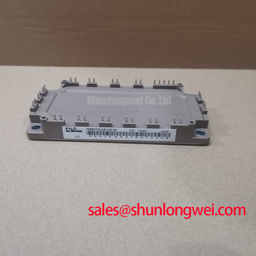
With the DC link discharged and isolated, first compare cold-state resistance between the main power terminals and inspect the terminal hardware, busbar faces, and baseplate contact area before fitting a 7MBR75VR120-56 into a failed power stage. This Fuji Electric power module is rated at VCES 1200 V and IC 75 A at TC 80°C, both Official Datasheet Specifications. The module is specified for a power-stage configuration described as 7-in-1, covering a three-phase converter, three-phase inverter, and brake function, with a 6-in-1 three-phase inverter-only configuration also identified in the official product information. Verify the original equipment schematic and terminal designation before any replacement work.
Before energizing the gate-drive board, trace each driver return from the existing controller to the module connection points. A separate auxiliary emitter return is often used in high-current IGBT assemblies to prevent the voltage developed in the main emitter path from being added to the gate-drive reference. Whether this topology is available in the actual equipment must be confirmed from its circuit diagram and the module terminal documentation; do not assume an auxiliary emitter connection from package appearance alone.
Design Consideration: keep the gate command loop physically separate from the high-current collector and emitter loop wherever the equipment layout permits. The purpose is to reduce mutual coupling during switching and to prevent gate ringing that may cause irregular turn-on or turn-off behavior. If a replacement board begins to show intermittent gate pulses, repeated driver alarms, or unstable collector-emitter waveforms, inspect the return path continuity, busbar clamping condition, and driver connector seating before changing gate-drive components.
| Official Specification | Condition | Value |
|---|---|---|
| Collector-emitter voltage | VCES | 1200 V |
| Continuous collector current | TC 80°C | 75 A |
| Collector-emitter saturation voltage | IC 75 A, VGE 15 V | 2.1 V typical, 2.7 V maximum |
| Operating junction temperature | Tj | Up to 150°C |
| Isolation voltage | AC, 1 minute | 2500 V |
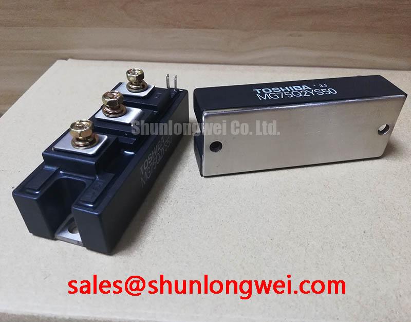
For repair teams evaluating a different physical power-stage arrangement, the 6MBI100S-140 can be reviewed as a separate module option. Its electrical function, terminal pattern, driver interface, cooling interface, and protection coordination must be checked against the original assembly rather than treated as a direct replacement.
7MBR75VR120-56 Circuit Protection & Reliability: Calibrating Isolated DC-DC Power Supply Sizing for High-Voltage Gate Drives
Check the isolated gate-drive supply at the driver board while the inverter remains disabled. The supply must retain adequate isolation performance and stable voltage under the actual switching common-mode environment. Isolation barrier capability and common-mode transient immunity are properties of the selected driver and isolated DC-DC supply, not published standalone specifications of the 7MBR75VR120-56. The system integrator should verify those requirements against the installed driver documentation and measured switching waveforms.
The module has an Official Datasheet Specification of 12.5 mJ per pulse Eon and 12.5 mJ per pulse Eoff, both stated at IC 75 A and VCC 600 V. These values support loss assessment only under the stated conditions. Actual inverter loss changes with current, DC-link voltage, gate control, temperature, switching frequency, and commutation-loop layout.
During waveform checks, observe the diode commutation interval as well as the IGBT transition. Reverse recovery behavior in the freewheeling path can interact with stray inductance and create ringing that appears as radiated noise or collector voltage overshoot. Design Consideration: keep the DC-link commutation loop compact and verify whether the original snubber network, laminated bus structure, and capacitor placement are still intact. A snubber should be evaluated from measured waveform behavior rather than added by a fixed rule.
Where a front-end or auxiliary converter stage is part of the same cabinet, technicians may also inspect the 6MBI450U-120A-05 as a separate power-semiconductor reference. Its ratings and topology must be assessed independently from this 1200 V, 75 A module. Fuji Electric’s power semiconductor technology resources provide manufacturer-level context for power-device integration.
Benchtop Waveform Tuning: Mitigating Stress via Fault-Clearing Dynamics: Type-I/II Desatur on 7MBR75VR120-56
Keep the first post-repair switching test controlled: use the equipment’s approved commissioning arrangement, monitor the collector-emitter waveform and gate-emitter waveform together, and confirm that the protection chain responds before sustained loading. The Official Datasheet Specification gives a short-circuit withstand time of at least 10 µs at VCC 600 V with VGE no greater than 15 V. It is not a permitted operating duration or a substitute for fast fault protection.
Desaturation protection is commonly used to identify an abnormal collector-emitter voltage rise while an IGBT is commanded on. Different driver architectures may classify fault behavior as Type I or Type II based on their sensing and response sequence. The relevant service task is to verify the complete delay path, including sensing, controller logic, isolation path, and gate discharge action, against the actual module protection limit and measured fault response.
Engineering Recommendation: use a controlled soft turn-off sequence when the driver architecture supports it, because abruptly removing gate drive during a high fault current can create inductive voltage stress. The correct response profile is determined by the inverter loop inductance, DC-link condition, protection circuit, and measured peak voltage. ⚠️ Field Alert: Never reconnect gate-drive plugs or probe power terminals until the DC link has been confirmed discharged and the controller lockout state is verified.
For commercial string inverter or micro-grid energy-storage maintenance, inspect the braking path as part of the fault-clearing review. The module’s stated 7-in-1 arrangement includes brake functionality, so an open braking resistor circuit, damaged connection hardware, or incorrect control sequence can affect DC-link behavior without proving that the IGBT module itself is defective.
Assembly Integrity & Layout Architecture: Implementing DC-DC Converter Interleaving and Ripple Current Control for 7MBR75VR120-56
Before tightening the module, clean the heatsink interface, inspect the baseplate for handling damage, and confirm that the mating surface is flat and free from old thermal compound residues. Design Consideration: apply thermal interface material as a uniform thin layer and tighten the mounting hardware in a staged cross pattern using the torque specified for the equipment’s fasteners and module mounting instructions. Uneven clamp force can create localized thermal resistance and distort later thermal measurements.
In bidirectional battery-linked systems, active power may move from the DC battery rack to the inverter link and back toward the storage side during charging or regenerative events. Interleaved DC-DC conversion can reduce ripple at system level, but its phase count, control behavior, capacitor stress, and current-sharing limits are system-determined. When integrating this module, engineers should verify DC-link ripple and junction-temperature excursion during the real peak-shaving profile rather than relying on nominal steady-state current alone.
Long motor cables require separate attention during inverter commissioning. Transmission-line reflections can raise the voltage seen at the motor terminals and alter the waveform observed at the module output. Confirm cable routing, output filtering, grounding practice, and measured terminal peaks under the intended switching condition. The module’s VRRM 1600 V repetitive peak reverse-voltage rating and IF(AV) 75 A average forward-current rating are Official Datasheet Specifications for the diode function, but complete cable and filter suitability remains an equipment-level verification.
For broader measurement and integration methods covering gate-drive loops, thermal interfaces, and converter topology checks, consult IGBT Design & Integration before approving full-load operation.