Content last revised on October 21, 2026
BSM150GXR120DN2 Identification and Initial Bench Checks
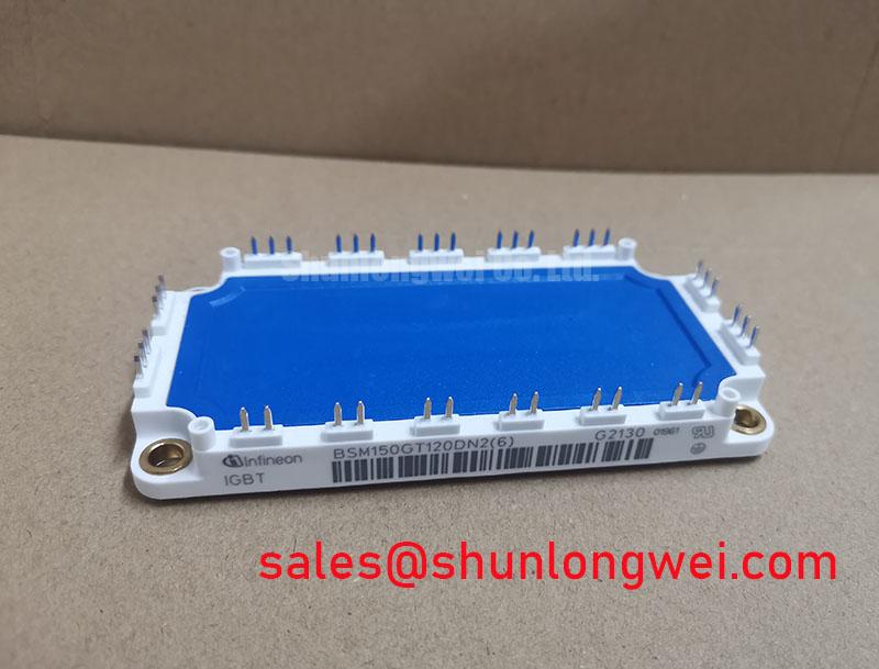
When a forklift traction inverter reports an overvoltage or gate fault, isolate the DC link, discharge the power stage, verify the absence of hazardous voltage, and compare the cold-state terminal behavior with a known-good assembly before applying drive pulses. The BSM150GXR120DN2 is an Infineon IGBT Module with a specified voltage rating of 1200 V and a rated collector current of 150 A under the applicable datasheet conditions. Its listed package is Module. These are manufacturer-level identification parameters; switching performance, thermal impedance, short-circuit capability, and gate-drive limits must be taken from the applicable device documentation and the completed system design.
For an incoming bench check, first confirm the printed part marking, terminal polarity, mounting condition, and isolation between power terminals and the module baseplate. With the module fully disconnected, a diode-test measurement across the appropriate antiparallel path can provide a comparative cold-state reading. The result is useful when matched against an approved reference unit, but a multimeter reading alone does not establish IGBT blocking integrity or dynamic switching safety. Keep the gate terminals at a defined reference during testing and use ESD controls throughout the inspection.
| Parameter | Value | Classification |
|---|---|---|
| Manufacturer | Infineon | Product identification |
| Part number | BSM150GXR120DN2 | Product identification |
| Rated voltage | 1200 V | Official specification |
| Rated collector current | 150 A, subject to datasheet conditions | Official specification |
| Package | Module | Official specification |
Benchtop Waveform Tuning: Mitigating Stress via Long Motor Lead Reflected Wave Voltage on BSM150GXR120DN2
Long motor cables can turn an otherwise acceptable inverter waveform into a terminal-voltage problem because cable impedance and the motor input do not behave as a lumped connection at fast switching edges. Reflections can add to the incident voltage at the motor or inverter terminals, and a measured spike approaching twice the applied DC-link voltage is a recognized transmission-line design concern rather than a guaranteed behavior of this particular module. The correct response is to capture the switching waveform at the relevant terminal with a properly rated differential probe and compare the result at several cable lengths and operating currents.
For the BSM150GXR120DN2, the 1200 V rating is an official device boundary, not a permission to operate continuously at the observed transient peak. Designers should evaluate the complete overshoot envelope, including DC-link tolerance, commutation effects, probe connection, stray inductance, motor cable routing, and the selected switching speed. The aim is to keep the peak voltage within the system’s verified semiconductor and insulation limits while preserving acceptable switching loss.
An output dv/dt filter or appropriately selected motor choke may reduce reflected-wave stress, but the selection must follow the motor-drive topology and measured waveform. Common-mode treatment addresses a different aspect of cable-related interference and should not be assumed to limit differential-mode reflected-wave voltage. A filter that reduces the edge rate can also change current ripple, control-loop behavior, acoustic noise, and semiconductor dissipation. During bench tuning, record collector-emitter voltage, phase current, gate-emitter voltage, and DC-link voltage at the same time. A ringing frequency that moves when the probe connection arrangement changes should be treated as a measurement setup issue until confirmed with a low-inductance connection.
Physical layout remains part of the voltage-control solution. Keep the high-current commutation loop compact, separate power and gate-drive returns, and avoid routing motor-phase conductors beside sensitive gate or fault-sense wiring for unnecessary distances. Clearance and creepage around the high-voltage terminals should be selected from the working voltage, pollution environment, insulation system, and applicable equipment standard. The module’s package designation alone does not define the finished inverter’s insulation rating.
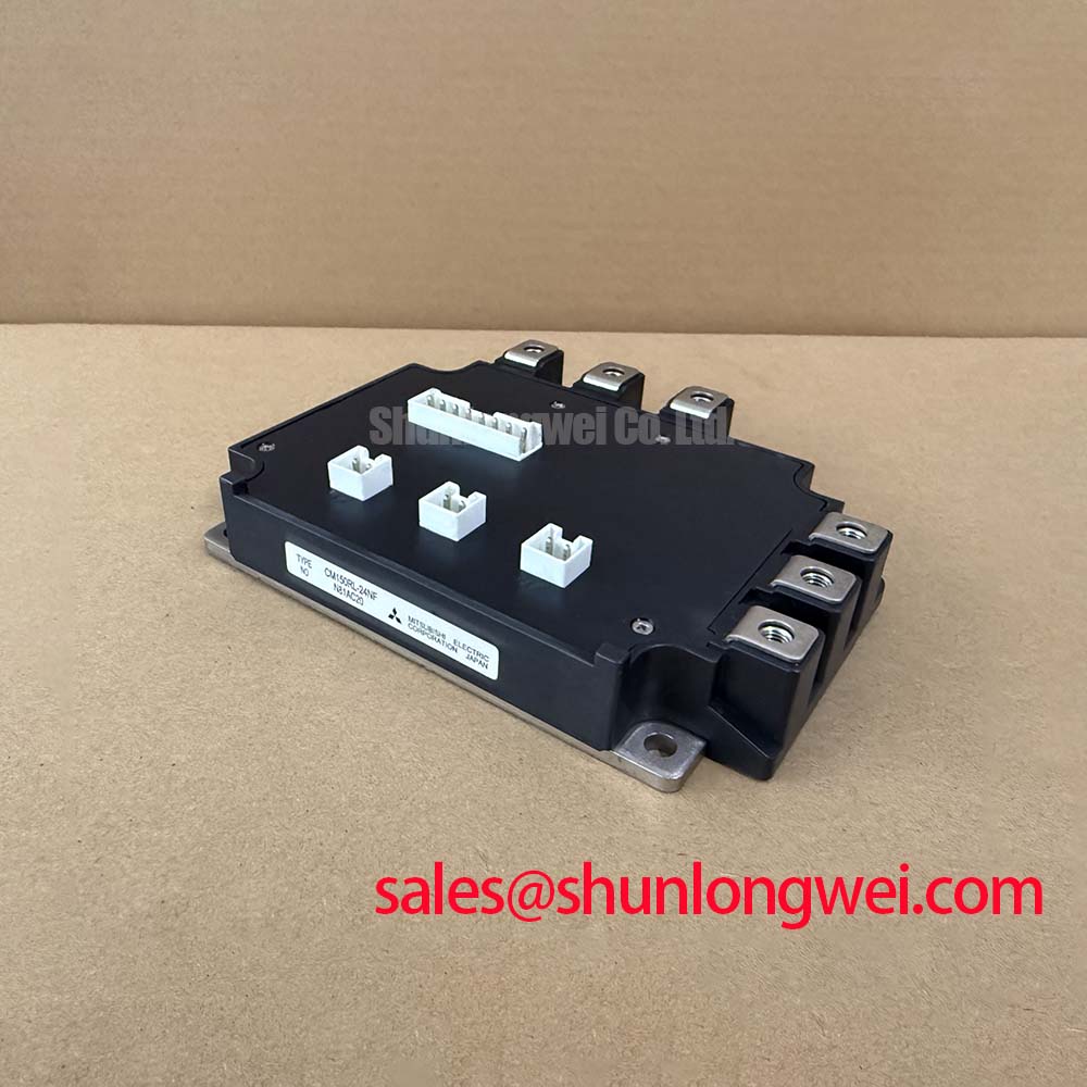
For a repair evaluation involving an electric material-handling vehicle or forklift traction inverter, compare the replacement module’s terminal arrangement, mounting footprint, gate-drive interface, and thermal path with the original assembly. The BSM300GB120DLC can be reviewed as a separate Infineon-related module option, but any substitution requires a pin-to-pin, electrical, mechanical, thermal, and protection review rather than a current-rating comparison alone.
💡 Bench Tip: Never connect or remove the gate-drive harness while the DC link or auxiliary gate supply is energized, and keep the first waveform test behind the system’s approved current and voltage interlocks.
Benchtop Waveform Tuning: Mitigating Stress via High dv/dt Cross-Conduction Shoot-Through on BSM150GXR120DN2
High dv/dt can couple through the inactive switch gate circuit and create an unintended gate excursion, especially when the driver return, emitter reference, and power commutation loop share avoidable impedance. In a half-bridge, that excursion can overlap with the commanded turn-on of the opposite device and produce cross-conduction. The waveform signature should be checked at the actual module gate and emitter terminals, not only at the driver board connector.
A dedicated low-impedance active Miller clamp is a useful design consideration when the switching environment produces a measurable false turn-on tendency. The clamp should be referenced to the local emitter return and remain effective during the interval in which the opposite device changes voltage. Gate resistance, driver output impedance, common-emitter inductance, dead time, and the physical gate loop all influence the result. Engineers should tune these elements together and confirm that the gate voltage remains controlled under the highest intended switching transition.
Negative gate bias is another possible design consideration for reducing susceptibility to dv/dt-induced turn-on. A system may evaluate a negative level in the region of −5 V to −15 V only when the selected driver, module gate-emitter limits, isolation supply, and turn-off transient behavior support it. This range is not an official rating supplied here for the BSM150GXR120DN2 and must not be treated as a default setting. The final value should be established from the applicable gate-drive documentation and oscilloscope verification.
High-side driver power integrity deserves the same attention as the gate waveform. If the design uses a bootstrap supply, its capacitor must supply the high-side driver’s gate-charge demand, quiescent current, leakage, and other applicable supply loads throughout the intended maximum high-side on-time while retaining adequate voltage at the driver output. The required capacitance is therefore determined from the driver data, the actual gate charge at the chosen gate voltage, refresh interval, temperature, and allowable supply droop. A larger capacitor does not automatically correct poor bootstrap diode behavior, excessive leakage, or an unsuitable duty-cycle pattern.
During tuning, monitor both upper and lower gate-emitter signals with isolated measurement equipment and verify the commanded dead time at the module terminals. A narrow unwanted pulse may be hidden by a long probe connection or by measuring only the driver output. If a fault appears only after the motor cable is connected, separate the gate-drive coupling investigation from the reflected-wave investigation by testing first with a controlled load and then with the installed cable arrangement.
External product families should not be used as proof of compatibility. Infineon’s information on OptiMOS™ low-voltage MOSFETs and EasyPACK™ modules is useful for understanding broader semiconductor and module technologies, but the gate-drive limits for this specific part must remain tied to its own documentation and measured application conditions.
BSM150GXR120DN2 Operational Boundaries: Evaluating SCSOA Overcurrent Protection: Implementing Limits
Short-circuit protection must interrupt the fault before the IGBT experiences an uncontrolled combination of high current, high voltage, and excessive junction temperature. A practical protection chain normally combines fast current or desaturation sensing, a defined fault blanking interval, gate inhibition, and a controlled turn-off path. The frequently discussed sub-10-microsecond response objective is a system engineering target for selected protection architectures, not an official SCSOA specification established by the basic product data provided here. The complete fault-clearing time must remain within the device’s documented short-circuit withstand capability under the applicable conditions; that capability must not be assumed from its voltage and current ratings.
Desaturation detection can identify an abnormal rise in collector-emitter voltage while the device is commanded on, but the sensing network must distinguish a genuine short circuit from normal switching overshoot, diode recovery, measurement noise, and insufficient gate drive. The fault threshold, blanking behavior, filter delay, and driver propagation time should be evaluated as one timing chain. A type-I or type-II short-circuit classification may be useful in the protection strategy, yet the classification criteria must come from the selected driver and the device application documentation.
Two-stage soft turn-off is commonly considered when an abrupt gate discharge would create excessive inductive voltage. The first stage reduces the current transition rate, while the second stage completes turn-off after the fault energy has been controlled. The resistor, current sink, gate clamp, and timing must be selected from the actual commutation inductance and measured collector-emitter overshoot. The principle is to limit the voltage peak without leaving the device in a high-loss state longer than the verified short-circuit withstand interval.
Transient thermal behavior belongs in the same evaluation. A short pulse can raise the junction temperature, so the calculation should use the applicable transient thermal impedance, actual pulse duration, starting temperature, switching state, and power waveform rather than only the steady-state thermal resistance. Such a calculation does not replace verification of the device’s short-circuit safe operating area. Peak junction-temperature margin is a system calculation that must include the heatsink interface, cooling condition, case temperature, and repeated fault sequence. No field lifetime or failure-rate value is established by the parameters listed for this product.
Mechanical assembly can undermine an otherwise suitable protection design. The baseplate must sit evenly against a clean, appropriate heatsink surface, with the thermal interface material applied according to the material supplier’s process. Excess compound can increase bond-line variation, while insufficient coverage can create local thermal resistance. Fastener sequence, washer selection, mounting flatness, and the torque specified by the module and heatsink documentation should be controlled in production; a generic torque value should not be presented as an Infineon specification for this model.
When a repaired traction inverter trips during acceleration, capture the fault timing, phase current, DC-link voltage, gate-emitter voltage, and collector-emitter voltage before changing protection thresholds. Inspect whether the fault begins at turn-on, during diode recovery, after cable reconnection, or during a mechanical load change. A protection trip can reflect several interacting conditions, so replacing the module without preserving the original waveform evidence may remove the most useful diagnostic information. For further discussion of switching-loop behavior and snubber evaluation, consult Mastering Power System Dynamics.