Content last revised on September 10, 2026
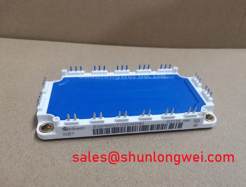
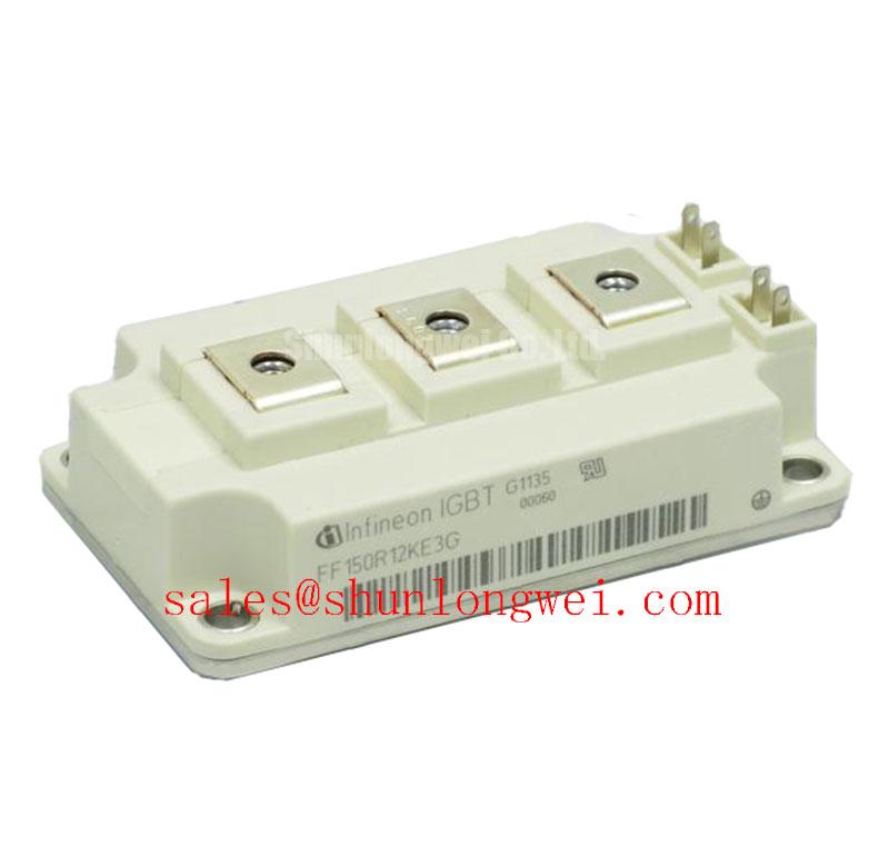
Begin incoming inspection by isolating the BSM150GAL120DLC, applying ESD controls, checking the module marking against the purchasing record, and measuring the accessible power terminals with a multimeter before any powered test. Confirm that the measured terminal relationships agree with the original circuit drawing, then verify the nameplate boundary of 1200 V voltage rating and 150 A current rating. These are the available official product specifications for this Infineon IGBT Module; pin polarity, internal circuit topology, isolation rating, switching limits, thermal resistance, and surge current capability should be confirmed from the applicable manufacturer datasheet before replacement approval.
BSM150GAL120DLC Thermal-Electrical Optimization: Suppression of 2x VDC Voltage Doubling at Practical Tuning
In a heavy-duty variable frequency AC motor drive, start the investigation at the DC link, inverter output terminals, motor cable, and any installed output filter. A long motor lead can behave as a transmission path rather than a simple resistive load. Reflections caused by impedance discontinuity may combine with the switching edge and produce a terminal overshoot that approaches twice the local DC-link voltage under unfavorable conditions. This is a system-level behavior, not an additional rating of the BSM150GAL120DLC.
Design Consideration: Treat the 1200 V rating as an official component boundary, not as permission to accept an uncontrolled switching spike. The system designer should measure the collector to emitter waveform directly at the module connection points with a suitable differential probe. Probe ground lead length, probe bandwidth, and the physical measurement loop can substantially alter the displayed overshoot. A second measurement at the motor-side filter or cable termination helps distinguish inverter commutation behavior from cable reflection.
Output chokes, dv/dt filters, and sine-wave filters should be evaluated from the motor insulation requirement, cable length, switching frequency, motor impedance, and drive control strategy. Their selection is an Engineering Recommendation determined by the complete drive, not by the module current label alone. The engineer should verify that the filter does not create excessive reactive current, resonance, or additional semiconductor stress during acceleration and regeneration.
A practical fault trace begins with a known-good low-power switching test. Compare the collector-emitter waveform during turn-off, then repeat the observation at the inverter output and at the motor terminals. If the overshoot changes significantly with cable arrangement or filter connection, investigate parasitic inductance and impedance mismatch before changing the gate-drive setting. Minimize the commutation loop area, keep the DC-link decoupling physically close to the switching path, and route the gate-drive return away from high-current switching copper.
A MOV or other coordinated clamping network may be considered as part of the overvoltage protection system. Its clamping level, energy capability, repetition duty, and fault behavior must be selected from the actual DC-link conditions and transient profile. A MOV should not be treated as a substitute for controlled layout, appropriate filtering, or measured switching margins. The complete assembly should be tested for peak voltage during hard switching, regenerative operation, motor disconnection, and abnormal load transitions.
The official information supplied for this product does not specify ITSM, short-circuit withstand time, gate voltage limits, or transient repetitive capability. Do not infer these values from the 150 A rating. During a replacement assessment, obtain the original drive service data and applicable Infineon documentation, then compare the existing protection sequence, current waveform, and thermal conditions with the verified module limits.
BSM150GAL120DLC Thermal-Electrical Optimization: PCB Gate Loop Layout Symmetry Practical Tuning
Before connecting a gate driver, identify every accessible gate, emitter, auxiliary emitter, collector, and control reference from the approved circuit drawing. A diode-mode reading can help reveal unexpected conduction paths, but it does not prove gate oxide integrity or dynamic switching health. Measure the device in a cold, unpowered state and compare the readings with a known-good unit of the same documented configuration. Avoid applying an uncontrolled external voltage to an unverified gate terminal.
For a high-current IGBT module, the gate loop should be treated as a low-noise control circuit. The main emitter path carries substantial switching current and produces voltage changes across its stray inductance. If the gate-drive return shares this path, emitter voltage movement can be fed back into the driver reference. This common-emitter coupling may appear as ringing, uneven turn-on, false turn-on, or abnormal gate plateau behavior. Separate the auxiliary control return from the main power emitter path wherever the verified module construction and terminal arrangement support that connection.
Design Consideration: Use a compact gate loop with closely coupled outgoing and return conductors, while keeping the control return physically separated from the highest di/dt power route. The required conductor geometry, copper width, isolation spacing, and damping network are system-determined. Confirm the result with simultaneous gate-emitter and collector-emitter oscilloscope traces rather than relying on a static resistance check.
When multiple modules are connected in parallel, symmetrical busbar geometry is important for both static and dynamic current sharing. Equal electrical path length, similar contact resistance, and matched gate-drive timing reduce the chance that one module carries a disproportionate portion of the pulse. IGBT forward voltage generally exhibits a positive temperature coefficient in the relevant high-current operating region, which can support static current sharing as temperature rises. That behavior does not automatically guarantee equal dynamic sharing during switching, where stray inductance, gate-loop coupling, driver mismatch, and layout asymmetry remain influential.
Parallel operation should therefore be validated with current-probe measurements on each branch. Compare turn-on current, turn-off current, collector-emitter voltage, and gate-emitter voltage under the intended load and temperature range. If one branch displays different ringing or switching delay, inspect busbar geometry, gate-return routing, driver output impedance, and mechanical contact conditions before modifying the control waveform.
Negative gate turn-off bias may be used in some industrial inverter designs to improve immunity to dv/dt-induced turn-on, but the suitable value and timing are not provided in the supplied official parameters for this model. The gate driver designer should verify the permitted gate-emitter voltage range from the applicable datasheet and evaluate negative bias against gate oxide stress, driver isolation, startup sequencing, and common-mode transients. Shielding or guard routing around the gate-drive reference can reduce capacitive pickup, but its effectiveness must be confirmed in the assembled drive.
For broader application context, engineers can consult the Industrial Applications guide when reviewing busbar arrangement, switching protection, and thermal integration principles. The Infineon IGBT Modules & Discretes Official Portfolio is also a useful reference for comparing documented module families without assuming that electrical ratings are interchangeable.
💡 Bench Tip: Keep the module and test leads at the same cold-state condition, protect the gate terminals from ESD, and record a known-good diode-mode and resistance baseline before applying any gate-drive signal.
Benchtop Waveform Tuning: Mitigating Stress via Calculating Failures-in-Time Rates in High Altitude on BSM150GAL120DLC
Do not assign a FIT rate, Single Event Burnout probability, or altitude derating value to the BSM150GAL120DLC without a traceable reliability source. The supplied official parameters identify a 1200 V voltage class, 150 A current class, and module package, but they do not provide neutron-flux data, SEB qualification results, FIT figures, or a high-altitude operating curve. Any numerical reliability prediction would require an applicable Infineon qualification document, test report, or recognized reliability methodology with stated assumptions.
At installations above 2000 m, atmospheric conditions can affect enclosure cooling, insulation coordination, and external clearances. Terrestrial neutron exposure is a separate reliability topic and should not be converted directly into a device failure rate by estimation. A responsible engineering review should identify the actual installation altitude, DC-link operating range, switching waveform, cooling arrangement, pollution environment, and insulation system, then obtain the relevant manufacturer and standards-based guidance.
For bench work, concentrate on measurable electrical stress. Capture collector-emitter peak voltage during turn-off, gate-emitter transients, current fall time, and the temperature at the module mounting surface. Repeat the test with the intended snubber, clamp, DC-link capacitor arrangement, and motor-side filter. The design objective is to preserve adequate voltage margin against measured transient peaks while the final margin remains a system-engineering decision.
When evaluating a possible SEB concern, inspect the complete event record rather than attributing a failed device to altitude alone. Review DC-link precharge, regenerative events, load interruption, gate-driver supply behavior, desaturation response, and the timing of the protection circuit. A transient may be produced by commutation inductance, a measurement artifact, an incomplete clamp path, or control instability. Correlate the oscilloscope record with the drive fault log and the physical condition of the external protection components.
Industrial designers may review the neutral technical information in the Infineon Automotive Qualified Power Modules resource for qualification terminology, but automotive qualification information should not be transferred to this industrial module without explicit product documentation. Likewise, the presence of an IGBT module in a drive does not by itself establish compliance with CISPR, EN 55011, safety, insulation, or EMC requirements. Those claims belong to the completed equipment and its verified test configuration.
If the original drive used a lower-current device, the BSM75GD120DLC may appear during a cross-reference review, but it must be evaluated objectively against topology, voltage, current, gate requirements, thermal path, package geometry, and protection settings. A lower or different rating is not an automatic replacement decision. The system integrator should validate every electrical and mechanical interface against the original equipment documentation.
BSM150GAL120DLC Thermal-Electrical Optimization: Thermal Paste Degradation Prevention and Mounting Practical Tuning
Inspect the heatsink, baseplate contact area, mounting holes, fasteners, and interface material before installing the module. Remove contamination without scratching the contact surface, check for visible distortion, and confirm that the module sits naturally on the heatsink rather than being pulled into position by uneven screw tightening. The supplied product data identifies the package as a Module, but does not provide baseplate flatness, mounting torque, thermal resistance, or an approved thermal interface material specification.
Thermal paste should form a continuous interface with minimal voiding while remaining thin enough to avoid creating an unnecessary thermal barrier. The appropriate application thickness is a Design Consideration governed by the paste manufacturer, surface finish, baseplate condition, and clamping method. Do not assume a commonly quoted thickness range is an Infineon specification for this model. Excess material can migrate toward nearby insulation surfaces, while insufficient material can leave dry contact zones.
Use a progressive and symmetrical fastening sequence so that contact pressure develops evenly across the baseplate. The required screw type, torque, washer arrangement, thread engagement, and final sequence should follow the module documentation and heatsink manufacturer instructions. After installation, inspect the interface for squeeze-out patterns where practical and verify that the electrical isolation system remains intact. Thermal paste aging should be investigated through temperature trend comparison, fan and airflow checks, heatsink cleanliness, and measured case-to-heatsink behavior rather than assumed service-life figures.
During thermal validation, record module case temperature, heatsink temperature, ambient conditions, switching current, duty cycle, and cooling-system status. Compare the result with the verified maximum semiconductor junction-temperature specification and applicable thermal-resistance data from the datasheet. If temperature rises gradually over repeated tests, examine interface condition, mounting pressure, airflow restriction, current imbalance in parallel branches, and switching loss. A thermal symptom can have several interacting causes, so the measurement sequence should preserve the original operating conditions.
🔧 Bench Diagnostic: Disconnect the DC link and wait for the verified discharge procedure before touching power or gate connections, then recheck the absence of hazardous voltage with an appropriate meter.
For procurement and repair records, retain the exact model identification, manufacturer documentation revision, approved circuit drawing, incoming cold-state measurements, installation method, and waveform results. The BSM150GAL120DLC should be released for a heavy-duty variable frequency AC motor drive only after its 1200 V and 150 A official ratings, mechanical fit, gate-drive interface, cooling path, protection network, and system-level test margins have all been checked against the original equipment requirements.