Content last revised on October 9, 2026
Dynamic Braking Chopper Operation & Regenerative Deceleration Energy Absorption
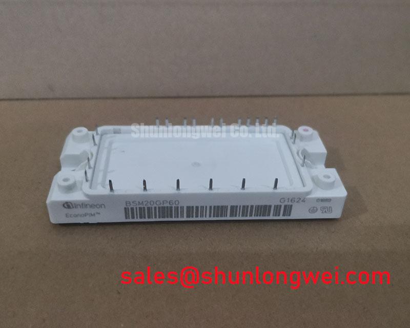
Before connecting the replacement, isolate the DC link, inspect the module body and terminals, and verify the nameplate boundary of 600.0 V and 20.0 A against the original drive documentation. The Infineon BSM20GD60DN2 is an IGBT Module in a module package. These are the official product parameters supplied for this product page; switching frequency, gate voltage, short circuit capability, thermal resistance, internal circuit arrangement, and terminal layout should be confirmed from the applicable manufacturer documentation before commissioning.
| Manufacturer | Infineon |
| Part number | BSM20GD60DN2 |
| Product category | IGBT Module |
| Rated voltage | 600.0 V |
| Rated current | 20.0 A |
| Package | Module |
For a precision stepper or BLDC servo actuator, begin the braking investigation at the complete DC link rather than at the IGBT alone. During rapid deceleration, motor energy can return through the inverter into the DC link. If the drive cannot absorb or return that energy, the link voltage rises and the braking chopper must control a ballast resistor or another approved energy path. The BSM20GD60DN2 provides the switching device under evaluation, while the resistor, DC-link capacitor, brake controller, current path, and thermal structure remain system-level decisions.
Confirm the motor inertia, maximum commanded speed, deceleration profile, repetition rate, and permitted DC-link voltage from the servo drive design file. The braking resistor must be assessed for both pulse energy and average thermal loading. A resistor that survives one emergency stop may still overheat during repeated positioning cycles. Designers should also check the resistor’s insulation system, mounting clearance, airflow, enclosure temperature, and connection inductance. The IGBT voltage rating must be compared with the measured switching peak, not only with the nominal DC-link value.
During commissioning, monitor the DC link with a properly rated differential probe and observe the chopper collector-to-emitter waveform during the most demanding stop command. A rising plateau followed by repeated overshoot may involve control timing, resistor wiring inductance, gate-drive behavior, or an incorrect braking threshold. Do not assign the symptom to the module without checking the command signal, gate waveform, DC-link ripple, and resistor temperature together. The measurement setup itself must be suitable for the voltage category and transient environment.
Physical spacing around the high-voltage terminals should follow the applicable insulation and creepage requirements for the actual working voltage, pollution level, enclosure, and altitude. Keep the braking loop compact, route power conductors so that the forward and return paths remain close, and prevent the gate-drive wiring from running parallel to the high-current collector path. A replacement assessment may include the neutral comparison unit FF150R12ME3G, but electrical, mechanical, thermal, and control compatibility must be verified rather than assumed.
When a resistor is switched externally, verify whether the controller expects a particular polarity, gate-drive reference, or fault response. The BSM20GD60DN2 product information supplied here does not establish a complete brake-controller topology. The integrator should therefore confirm terminal identification, internal circuit configuration, switching limits, and protection requirements from the original Infineon documentation before applying power.
Active Miller Clamp Implementation & Parasitic Capacitive Turn-On Prevention
High-voltage servo inverters can transfer a transient current through the opposing device’s Miller capacitance when the complementary switch changes state quickly. That current can lift the inactive gate and create unintended conduction. For a half-bridge using the BSM20GD60DN2, the gate-driver layout should place the driver return, gate path, and emitter reference close together. The final loop geometry, gate resistance, dead time, and switching speed must be established from measured waveforms and the complete inverter design.
An active Miller clamp is a design option when the driver supports it and when the module’s gate-emitter behavior is compatible with the selected driver. The clamp should engage after the gate has been discharged and hold the gate at a low impedance during the opposing transition. If the driver uses a negative off-state bias, values such as −5 V to −15 V are Design Considerations only; they are not official BSM20GD60DN2 parameters supplied in this product brief. The system engineer must verify the permitted gate-emitter voltage, driver isolation, UVLO behavior, and transient immunity from the relevant datasheets.
Check the gate waveform directly at the module terminals, not only at the driver output. Probe ground lead inductance can create a false gate spike or conceal the real one. Compare the inactive gate voltage with the collector-emitter transition of the opposite switch. A brief rise may result from Miller current, common-emitter inductance, insufficient clamp strength, excessive gate-loop impedance, or measurement error. A controlled increase in gate resistance may reduce ringing, but it also changes switching loss and should be evaluated with thermal measurements.
Line-frequency ripple on the DC link can change the switching stress across the servo operating range. Test at the lowest and highest expected supply conditions, including regenerative operation and rapid direction changes. An RC snubber can reduce a measured high-frequency transient when its capacitance, resistance, pulse current, insulation, and dissipation are selected from the actual waveform. It should not be installed as a generic cure without identifying the ringing frequency and its current path.
Any adjacent rectifier or front-end device affects the shared DC-link behavior. Engineers evaluating a related system topology may review BSM100GAL100D as a separate component reference, while keeping the braking switch, rectifier, capacitor bank, and gate driver within their own verified electrical boundaries. The external Infineon Technologies resource should be consulted for current manufacturer documentation and application information.
💡 Pro Tip: Capture the gate-to-emitter waveform at the module pins during both turn-on and turn-off before changing the driver setting; an apparently harmless gate spike can be a probing artifact or a real cross-conduction risk.
Kelvin Emitter Connection & Parasitic Inductance Minimization in High-Speed Switching
A Kelvin emitter connection separates the low-current gate-driver return from the high-current emitter path. This arrangement can reduce the voltage error created when the load current changes rapidly, allowing the driver to sense a cleaner emitter reference. Whether the BSM20GD60DN2 provides a dedicated auxiliary emitter terminal cannot be established from the limited official parameters supplied here, so the original terminal drawing must be checked before designing a Kelvin return.
If an auxiliary emitter is available, route it directly to the driver reference and keep it separate from the main power emitter copper until the intended connection point. Do not share a narrow connector pin, long jumper, or high-current screw path with the gate-return circuit. If no auxiliary terminal is provided, the designer should minimize the common emitter segment and validate the resulting common-inductance voltage during switching tests. The objective is to reduce mutual coupling, not to impose a universal trace dimension or unverified inductance limit.
For precision motion equipment, switching behavior should be checked at low speed, rated speed, acceleration reversal, and regenerative braking. Observe collector-emitter voltage, gate-emitter voltage, phase current, and DC-link voltage with synchronized probes. Oscillation that appears only during a current reversal may originate in the commutation loop, motor cable, current sensor, DC-link capacitor placement, or control timing. A module replacement does not automatically remove those external causes.
Maintain physical separation between power terminals and control connectors in accordance with the insulation design. Avoid routing encoder, resolver, Hall, or current-sense wiring alongside the collector or emitter loop. Shielding and grounding arrangements are system-dependent and should be verified against the drive’s EMC test plan; the individual module must not be represented as independently certified to a complete equipment EMC standard.
Thermal installation also affects electrical repeatability. The mounting surface should be clean, flat, and mechanically stable, with the specified interface material applied according to the heatsink and module manufacturer’s instructions. Fastener sequence and torque should follow the applicable mechanical documentation. Uneven clamping can increase thermal resistance or stress the module base, while excessive force can damage the package or distort the mounting surface.
When comparing the BSM20GD60DN2 with another module, match more than voltage and current labels. Confirm circuit topology, terminal spacing, gate-drive reference, isolation requirements, thermal interface, mechanical envelope, and protection behavior. The linked Field Engineer’s Handbook provides a separate engineering reference for structured testing and failure analysis.
Mitigating Hard Switching Transients via Active Desaturation Soft Shutdown
A desaturation protection circuit can detect an abnormal rise in the conducting switch voltage and command a controlled turn-off. In a servo inverter, this protection must distinguish a genuine overcurrent event from a normal switching transient, diode recovery event, blanking interval, or measurement disturbance. The BSM20GD60DN2 data supplied for this page does not specify an internal desaturation circuit or a guaranteed short-circuit withstand time. External protection therefore requires validation with the selected gate driver and the actual module circuit.
Some industrial gate drivers use a two-stage response: an initial controlled reduction of gate current followed by a stronger shutdown after the fault is confirmed. This can reduce the voltage overshoot associated with abruptly interrupting a high current. The protection designer must set detection delay, blanking behavior, soft-shutdown strength, fault latch action, and reset logic from the driver documentation and measured short-circuit waveform. A target such as less than 10 microseconds is a Design Consideration from the requested application outline, not an official rating for this product.
Test the protection circuit with a controlled, current-limited method before connecting the motor and full DC-link energy. Confirm that the desaturation pin remains stable during normal turn-on, that the fault signal reaches the controller, and that the driver supply does not collapse during shutdown. Measure the collector-emitter overshoot at the module terminals and compare it with the verified voltage boundary. The gate-driver isolation barrier, fault propagation path, and controller response should be assessed as one protection chain.
Hard-switching transients are strongly affected by stray inductance in the DC-link capacitor connection, phase-leg busbar, emitter return, and probe loop. Keep the commutation path compact, place suitable high-frequency decoupling close to the switching bridge, and verify the current-sharing path under the real mechanical assembly. Snubbers, clamps, and active gate control may reduce overshoot, but their values must be selected from measured energy, pulse repetition, temperature, and insulation requirements rather than copied from an unrelated module.
Before releasing a repair unit, inspect solder or screw terminals, confirm the gate polarity and reference, check isolation with an approved procedure, and perform a low-energy switching test. Then repeat the test across the intended DC-link range, motor current range, acceleration profile, and braking cycle. Record the gate waveform, switching-node waveform, fault timing, heatsink temperature, and DC-link response so that later service work can distinguish an electrical installation issue from a component issue. Product information and application guidance from Infineon HybridPACK™ Drive may provide useful comparative context, but it does not replace the documentation for the BSM20GD60DN2.