Content last revised on September 18, 2026
Incoming Inspection and Preliminary Checks for BSM50GD120DN2E3226
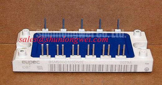
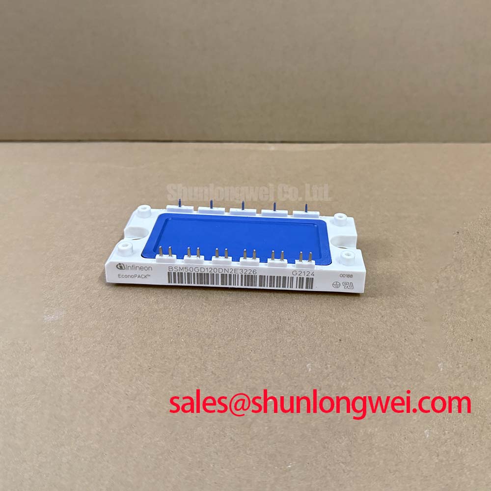
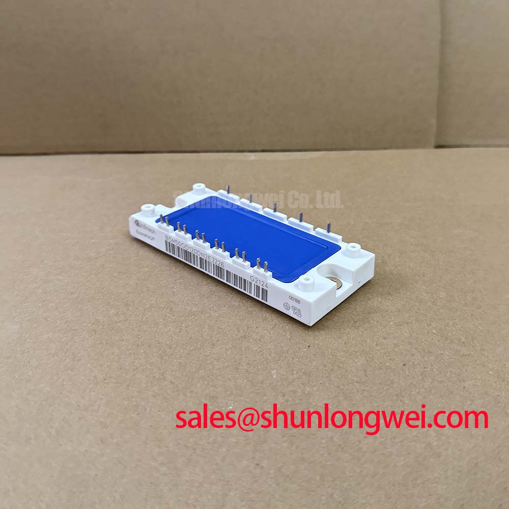
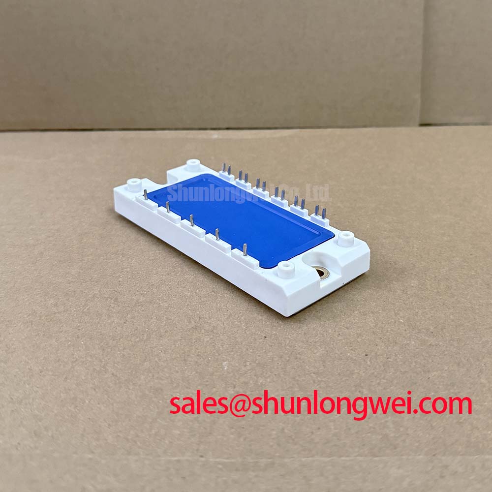
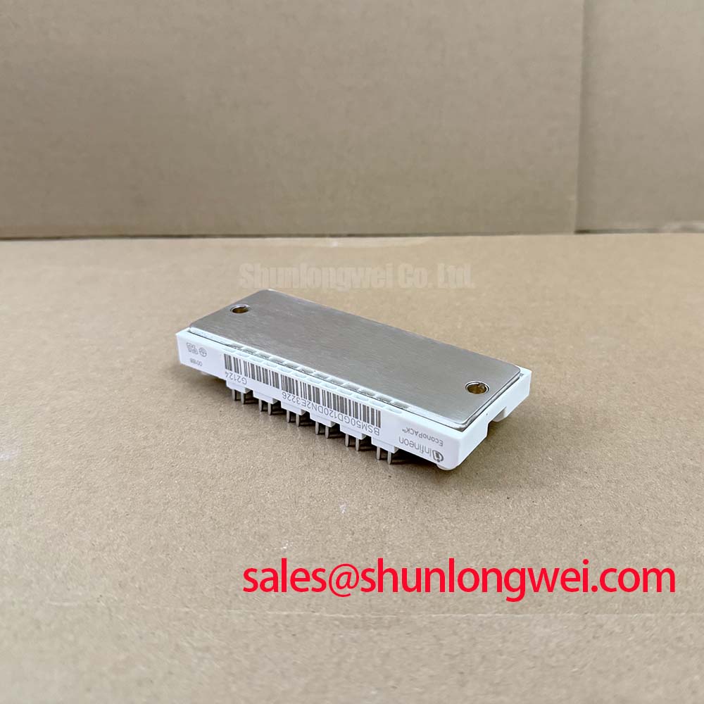
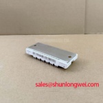
With the equipment isolated and the DC link confirmed discharged, begin incoming inspection of the BSM50GD120DN2E3226 by checking the module case, terminals, and mounting surface for transport damage, contamination, or signs of uneven prior clamping. This Infineon power semiconductor is a 1200 V, 50 A IGBT Module according to the available official product specification. Before fitting it into an industrial inverter welder or medium frequency induction heating supply, compare the module marking, terminal arrangement, and external dimensions with the removed unit and the original equipment documentation.
| Parameter | Value | Classification |
|---|---|---|
| Manufacturer | Infineon | Official product identification |
| Collector emitter voltage rating | 1200 V | Official Specification |
| Current rating | 50 A | Official Specification |
| Package format | Module | Official Specification |
Cold checks are useful for identifying obvious installation risks before power is applied. With the gate circuit disconnected from its driver, use a meter diode function only as a comparative screening tool between corresponding power terminals and against a known good assembly where one is available. A reading that differs substantially from the reference may justify further investigation, but it does not independently establish switching capability. The original Infineon documentation remains necessary for terminal assignment, gate limits, diode characteristics, switching behavior, thermal data, isolation requirements, and approved mounting conditions.
Field Diagnostics & Commissioning: Dynamic Gate Impedance Control for Robust BSM50GD120DN2E3226 Topologies
For a BSM50GD120DN2E3226 installed in a bridge or chopper position, commissioning should begin at the driver interface rather than at full power. Confirm that each driver output reaches the intended gate and its designated emitter reference, then inspect the driver return path for shared high current copper. A gate that appears correct at the controller connector can behave differently at the module when switching current returns through the same conductor as the power emitter path.
Dynamic gate impedance is a system level property. It includes the driver output stage, series gate components, wiring or PCB routing, the module terminals, and the local power loop. Design Consideration: minimize the area of the gate drive loop so that rapid collector voltage movement is less able to disturb the gate reference. Where the original drive board employs an active Miller clamp or a controlled off state, retain its intended topology during repair unless the system design has been reviewed and tested.
A negative off state is sometimes used in industrial gate driver circuits to improve immunity to induced turn on. It is not an official operating requirement stated by the supplied product data for this module. When integrating a replacement, the system engineer should verify the permitted gate drive range from the manufacturer documentation and observe the actual gate to emitter waveform at the module terminals. An unexpected rise in off state gate voltage can indicate return path coupling, unsuitable impedance, an isolation problem, or a probing arrangement that is influencing the measured signal.
During first energization, check the DC link, gate command, and output current with the load condition controlled by the equipment procedure. Do not treat a clean low voltage test as proof of acceptable operation at production voltage. Switching overshoot, ringing, and cross conduction risk depend on the completed busbar, capacitor placement, snubber network, cable arrangement, and driver behavior.
💡 Bench Tip: Keep ESD protection in place and record cold state terminal comparisons before disconnecting a gate lead, because a floating gate can make later measurements difficult to interpret.
Transient Dynamics & Electrical Design: Optocoupler vs Digital Coreless Transformer on BSM50GD120DN2E3226
The isolation technology on a driver board must be assessed as part of the complete converter, not selected from the module voltage rating alone. Optocoupler based drivers and digitally isolated driver architectures can both be encountered in repairable inverter welders and induction heating equipment. Their suitability depends on the isolation barrier rating, transient immunity, supply arrangement, propagation behavior, fault response, PCB creepage and clearance, and the characteristics specified by the driver manufacturer.
The 1200 V collector emitter rating is an Official Specification of the module. It should not be interpreted as a stand alone statement of the gate driver isolation barrier. Designers should verify reinforced or functional isolation requirements against the equipment insulation architecture and applicable safety documentation. They should also verify that the selected isolator retains adequate immunity to the common mode voltage transitions actually measured in the converter.
Complementary switch commands need an interlock that prevents both devices in a switching leg from receiving an effective on command at the same time. Design Consideration: establish dead time from the measured turn off and turn on behavior of the actual driver, module, DC link layout, operating temperature, and load. A fixed value copied from another power stage can leave inadequate separation or impose unnecessary distortion on the output waveform.
Oscilloscope checks should reference the intended local gate emitter pair. A long ground lead or an unsuitable probe connection can capture bus noise rather than the real gate condition. If a replacement driver board is being evaluated, compare its command timing and fault behavior with the existing control scheme before connecting the main power stage. Infineon’s IGBT modules and discretes portfolio and its IGBT modules overview provide useful manufacturer context when reviewing power semiconductor families, but module specific limits must come from the relevant product documentation.
In an equipment chain that includes an input or auxiliary conversion stage, the BSM75GB120DN2 can be reviewed as a separate associated module. Its electrical ratings, terminal mapping, gate drive needs, and thermal interface must be evaluated independently; its presence does not establish compatibility with the BSM50GD120DN2E3226.
Assembly Integrity & Layout Architecture: SCSOA Overcurrent Protection for BSM50GD120DN2E3226
Short circuit protection must be treated as a driver and system protection function. The supplied official data identifies this product as a 1200 V, 50 A IGBT module, but it does not provide a short circuit safe operating area duration, detection threshold, or soft turn off profile. Those values must not be inferred from the current rating or borrowed from a visually similar module.
In practical fault analysis, inspect how the driver detects excess current or desaturation, how it blocks further turn on commands, and how it removes gate charge after a fault. A controlled fault turn off path can reduce stress caused by inductance in the DC link and output loop, but its implementation is system determined. Designers should validate peak voltage at the module against the DC link condition during switching and fault tests, using approved safety procedures and appropriately rated instrumentation.
Mounting integrity affects both thermal transfer and electrical repeatability. Clean the mating surfaces, use the hardware and torque requirements defined for the specific module and heatsink assembly, and avoid forcing the module into a warped interface. The module case should sit evenly on the heatsink before final tightening. Thermal compound quantity, clamp sequence, and power terminal connection details are assembly controls that should follow the original equipment procedure or the module manufacturer’s instructions.
A metal oxide varistor or other surge suppression network may be present elsewhere in an industrial power supply. Design Consideration: review it as part of the full transient path, including fuse coordination, DC link capacitors, snubber parts, contactors, and wiring. A surge component cannot be assumed to protect every switching event, and any replacement should be assessed against its own documented voltage, energy, and safety characteristics.
Where a higher current module is being considered during a service evaluation, BSM75GD120DLC is a related Infineon module reference that can be examined. It is not an automatic replacement for the BSM50GD120DN2E3226. The technician should verify package dimensions, terminal positions, gate drive requirements, thermal performance, protection settings, and the complete converter qualification plan before making any substitution decision.
BSM50GD120DN2E3226 Circuit Protection & Reliability: Calibrating Auxiliary Emitter Return Trace Separation
Do not assume an auxiliary emitter or Kelvin emitter connection from the part number alone. Before routing or reconnecting a driver lead, verify every terminal designation from the original module drawing and equipment schematic. If the documented module interface includes a separate driver emitter reference, it should be routed back to the driver reference as intended instead of being merged casually into a high current emitter return.
Design Consideration: separating a sensitive gate driver return from the main switching current path helps reduce mutual coupling. This matters because voltage developed across shared inductance can alter the effective gate to emitter voltage during fast current transitions. The goal is not a universal trace geometry or a copied layout dimension. It is a verified low noise reference path that is checked at the module under the converter’s actual operating conditions.
When unexplained ringing, irregular current sharing, or repeated driver fault indications occur, inspect the physical return route before changing gate components. Look for loose terminal joints, shared return copper, altered busbar spacing, poor capacitor connections, and repairs that have moved the driver reference away from its intended point. If multiple modules are paralleled, static device matching alone cannot establish dynamic current sharing. The gate paths, power paths, thermal interfaces, and timing behavior need system level verification.
For broader troubleshooting methods covering gate drive, thermal management, and circuit topology interactions, consult IGBT Design & Integration. Apply those principles only after confirming the specific terminal arrangement and official limits of the BSM50GD120DN2E3226 within the repaired equipment.