

Content last revised on October 2, 2026
BSM50GX120DN2 Thermal Electrical Optimization: Symmetrical Busbar Geometry for High Current Practical Tuning
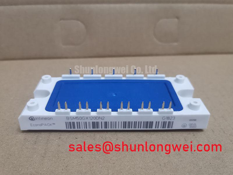
Before energizing a replacement, inspect the module body and terminals, confirm the nameplate against the failed unit, and record the cold state resistance between the relevant power terminals without applying a control signal. The BSM50GX120DN2 is an Infineon IGBT Module with an official rated voltage of 1200.0 V, an official rated current of 50.0 A, and a Module package designation.
| Manufacturer | Infineon |
| Model | BSM50GX120DN2 |
| Rated voltage | 1200.0 V, Official Specification |
| Rated current | 50.0 A, Official Specification |
| Package | Module, Official Specification |
These three confirmed data points establish the initial procurement and compatibility screen. They do not, by themselves, confirm switching frequency, short circuit withstand time, gate voltage limits, thermal resistance, isolation rating, internal circuit topology, or pin assignment. The system integrator should verify those details against the applicable Infineon documentation and the original equipment drawing before installation.
When this module is evaluated in a commercial string inverter or microgrid energy storage converter, begin with the physical current path rather than the control software. Compare the replacement terminal arrangement with the original assembly drawing, then inspect busbar contact faces for uneven pressure, oxidation, burrs, and evidence of localized heating. A module rated at 50.0 A still depends on the complete switching leg, conductor geometry, cooling arrangement, protection system, and operating profile for its usable current capability.
Design Consideration: A symmetrical busbar arrangement can help reduce unintended differences in stray inductance and current path resistance between parallel switching positions. Keep high current paths short and physically consistent, route gate wiring away from collector and emitter power transitions, and avoid allowing one phase leg to use a visibly longer return path than its counterpart. These are system layout principles, not additional factory specifications for the BSM50GX120DN2.
Static current sharing and dynamic current sharing require separate checks. The temperature behavior of IGBT conduction voltage should be confirmed from the manufacturer’s electrical curves before using any positive temperature coefficient assumption in a parallel design. During commissioning, measure phase current under the same command and load conditions, then compare waveform timing, overshoot, and ringing at the switching nodes. If one branch carries a different share, inspect gate loop symmetry, emitter return routing, busbar contact pressure, current sensor placement, and driver propagation timing before attributing the condition to the module itself.
For a replacement in a photovoltaic string inverter or battery converter, verify the DC link voltage, modulation method, switching frequency, gate driver supply, protection delay, and cooling path as a complete system. The official 1200.0 V rating is a component boundary, not permission to operate at an unverified DC link level. Peak switching voltage must be observed with suitable high voltage measurement equipment while the converter is tested across its intended load range.
Infineon’s IGBT Modules Overview provides useful manufacturer level context for module selection and application review. It should be read together with the exact device documentation because family level information cannot substitute for model specific electrical and mechanical data.
Field Diagnostics and Commissioning: Negative Gate Bias versus Active Miller Clamping in BSM50GX120DN2 Topologies
After confirming the power terminals and cooling installation, isolate the gate driver supply and inspect the gate emitter reference at the module connector. A gate signal that looks correct at the driver board may appear different at the module because of common emitter inductance, connector impedance, cable routing, or probe grounding. Use a differential measurement method appropriate for the voltage environment and compare the signal at the module terminals with the known good phase path.
Negative gate bias and active Miller clamping are external driver design options, not confirmed internal features of the BSM50GX120DN2. A negative turn off level must never be applied simply because it is common in another IGBT platform. The system designer should verify the permitted gate emitter voltage, driver isolation, power supply transient behavior, and gate resistor arrangement from the applicable Infineon documentation. If a negative bias is considered, its suitability must be validated during turn on, turn off, fault shutdown, and power sequencing tests.
Active Miller clamping can be considered where high dv/dt creates an unwanted gate voltage excursion during the opposite switch transition. The clamp loop should be physically close to the gate emitter reference and separated from the high current commutation path. If the measured gate waveform shows a transient excursion, do not assume cross conduction is the only possible cause. Check probe technique, common reference inductance, driver saturation, dead time, gate resistor condition, and the switching node waveform together.
Phase angle control and line frequency ripple can alter the thermal and electrical stress seen by the module. During commissioning, record gate voltage, collector emitter voltage, phase current, heat sink temperature, and fault timing at representative operating points. For a commercial inverter, the DC link control loop and the AC current command should be checked together because a ripple component can change pulse width, switching events, and instantaneous device loss.
An RC snubber may be evaluated when switching node ringing remains after the busbar and gate loop have been corrected. Its values are system determined and must be selected from measured ringing frequency, damping behavior, capacitor pulse capability, resistor energy, insulation spacing, and thermal performance. Do not treat a snubber as a universal cure for excessive overshoot. The final design should verify peak voltage against the 1200.0 V device rating and the complete transient margin under the intended switching conditions.
Field Alert: Disconnect the DC link and follow the equipment discharge procedure before unplugging the gate or auxiliary wiring from the module.
Field Diagnostics and Commissioning: Dynamic Power Loss Dissipation and Multi R in BSM50GX120DN2 Topologies
Thermal investigation should begin with measured switching and conduction behavior, not with a temperature limit copied from a different module family. The BSM50GX120DN2 has an official package designation of Module, but the supplied product data here does not establish a specific junction to case thermal resistance, transient thermal impedance curve, maximum junction temperature, overload duration, or case geometry. Those values must be taken from the applicable technical documentation before a thermal model is used for acceptance decisions.
A transient thermal impedance network can be useful for pulsed operation when its resistor capacitor branches are fitted to the manufacturer’s published data. In practical terms, the engineer converts measured or calculated instantaneous power into a time varying junction temperature response, then compares the predicted peak with the documented junction temperature boundary. A multi branch model is only an engineering calculation; it is not a measured field lifetime result and should be checked against temperature measurements under representative pulse patterns.
For a failed inverter leg, capture the current and voltage waveforms at turn on and turn off, estimate switching energy from the measured overlap, and separately examine conduction loss during the active portion of the cycle. Check whether the cooling interface, air or liquid flow, heat sink flatness, and sensor location match the original assembly. A temperature sensor mounted away from the module case can show a stable reading while the semiconductor junction experiences a short duration thermal peak.
Repeated overload events require an examination of the protection sequence. Desaturation detection, soft turn off, gate driver supply undervoltage behavior, fault latch timing, and controller restart logic should be reviewed as one chain. The BSM50GX120DN2 model information supplied here does not verify a particular short circuit safe operating area, desaturation threshold, soft shutdown profile, or short circuit withstand time. Designers should obtain those limits from the relevant manufacturer documentation and verify them with controlled tests.
High altitude operation, cosmic ray effects, single event burnout, FIT values, and service life cannot be assigned numerical margins from the basic voltage and current data alone. These subjects require authoritative device data, application notes, environmental assumptions, and an equipment level reliability method. For background on IGBT construction, electrical behavior, and application principles, consult The Ultimate IGBT Knowledge Base without treating general technical discussion as a model specific reliability guarantee.
Where multiple modules are used in parallel, compare electrical path length, gate drive timing, thermal coupling, and current measurement location. Infineon’s IGBT Paralleling Application Note offers manufacturer technical guidance for reviewing parallel operation. Any final current sharing result remains dependent on the complete converter layout and operating conditions.
Transient Dynamics and Electrical Design: Baseplate Thermal Grease Layer Control on BSM50GX120DN2
Remove the failed module and inspect the mounting surface before preparing the replacement. The heat sink should be clean, flat within the equipment manufacturer’s specified tolerance, and free from burrs that could create a local pressure point. Check the module base area for contamination or mechanical damage, then confirm that the mounting holes and terminal positions match the original mechanical drawing. The supplied product data confirms a Module package but does not provide baseplate dimensions, hole pattern, surface flatness, or mounting torque.
Thermal interface material should be applied as a continuous, even film that fills surface irregularities without creating excessive hydraulic resistance between the module and heat sink. The correct application amount depends on the selected compound, surface finish, flatness, pressure distribution, and equipment assembly procedure. Follow the TIM supplier and original equipment instructions, then inspect the spread pattern after a controlled trial installation if the service procedure permits.
Sequential tightening is a practical design consideration for achieving even contact pressure. Use the fastener pattern and torque sequence specified by the equipment manufacturer, and account for screw size, washer type, thread condition, spring hardware, and heat sink construction. A disc spring or other compliant washer can help maintain clamping force, but its installed height and load must be verified from the mechanical design rather than assumed from general practice. Double sided cooling, if present in the equipment, requires the pressure path and insulation stack to be verified independently on each side.
After mounting, inspect for displaced compound, rocking contact, tilted hardware, or a fastener that reaches bottom before applying pressure. Recheck terminal alignment before connecting laminated busbars. Power connections should be tightened according to the equipment or fastener manufacturer’s specification, while the control connector should be secured without transferring cable force to the module terminals.
Commission the repaired assembly at controlled load and monitor case temperature, heat sink temperature, phase current, switching waveform, and fault records. If temperature rises unevenly across equivalent phases, compare TIM spread, clamping pressure, airflow, sensor placement, gate timing, and current sharing. This measurement sequence distinguishes a thermal interface problem from an electrical imbalance without assigning a single cause from one symptom.
For procurement and technical cross checking, the BSM75GD120DLC is a separate Infineon module listing and should be evaluated only through its own voltage, current, topology, mechanical, gate drive, and thermal documentation. It should not be treated as an automatic substitute for the BSM50GX120DN2.