Content last revised on September 10, 2026
CM100DY-28H Ratings and Pre-Commissioning Checks
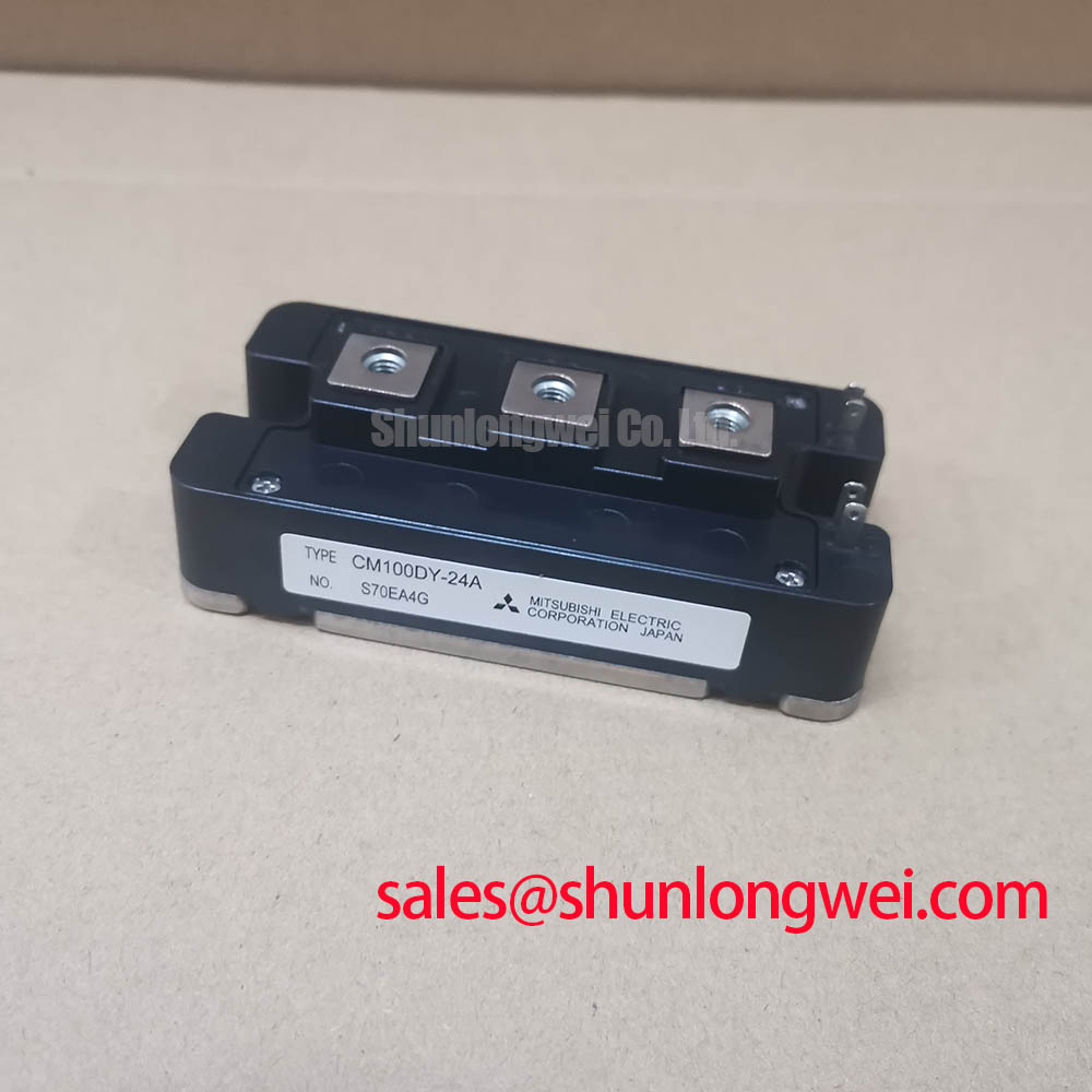
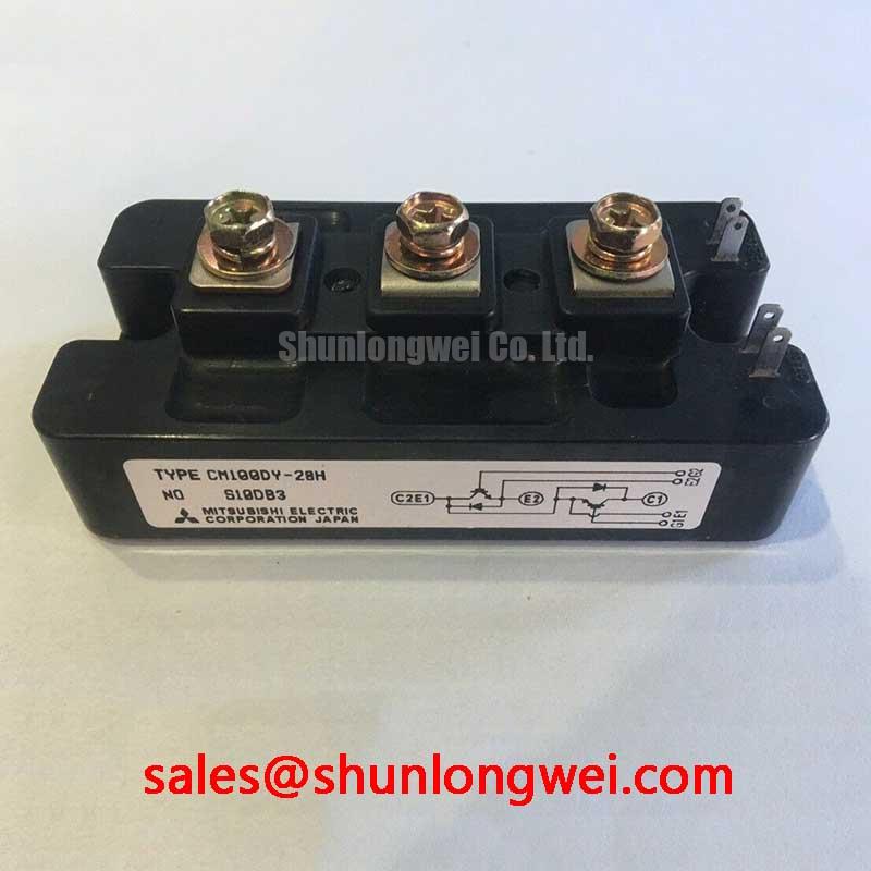
With the DC link discharged and the gate driver isolated, verify the module marking and compare the installed electrical boundary with the CM100DY-28H official ratings before reconnecting an industrial inverter welder or medium frequency induction heating power supply. This Mitsubishi dual IGBT module is rated at VCES 1400 V, IC 100 A at TC 25°C, and ICP 200 A for 1 ms, all Official Datasheet Specifications. Its gate emitter rating is VGES ±20 V; the driver must therefore be examined as part of the repair, rather than treating the power module as an isolated replacement item.
The module’s specified collector emitter saturation voltage is 2.2 V typical and 2.7 V maximum at IC 100 A under the datasheet test conditions. Maximum collector dissipation is 540 W at TC 25°C. These figures establish the device identity and give maintenance teams a factual basis for checking whether the existing cooling path, gate drive arrangement, and protection logic remain appropriate after a module change.
| Official Datasheet Specification | Rated Value |
|---|---|
| Collector emitter voltage, VCES | 1400 V |
| Continuous collector current, IC, TC 25°C | 100 A |
| Pulsed collector current, ICP, 1 ms | 200 A |
| Gate emitter voltage, VGES | ±20 V |
| Collector emitter saturation voltage, VCE(sat), IC 100 A | 2.2 V typical, 2.7 V maximum under the datasheet test conditions |
| IGBT junction to case thermal resistance per arm | 0.19 °C/W |
| Free wheel diode junction to case thermal resistance per arm | 0.38 °C/W |
| Diode reverse recovery time, IE 100 A | 0.15 µs typical under the datasheet test conditions |
Field Diagnostics & Commissioning: Negative Gate Bias and Active Miller Clamp in CM100DY-28H Topologies
Before commissioning, inspect the gate command at the module terminals with the intended power stage disconnected where practical. In inverter welders and induction heating supplies, rapid collector voltage movement can couple through IGBT capacitances and disturb a nominally off gate. A gate waveform that rises unexpectedly during the opposite switch transition may indicate common emitter inductance, excessive gate loop impedance, poor driver return routing, or inadequate control of the Miller current. It should be compared against a known good phase or a validated driver waveform, not judged from a single trace alone.
CM100DY-28H has an official typical gate emitter threshold voltage of 5.5 V under the datasheet test conditions. Threshold voltage is not a recommended operating gate drive value and should not be used as a field setting. Design Consideration: a negative off state gate bias and an active Miller clamp are commonly evaluated where switching conditions create a risk of induced turn on. A negative bias range of minus 5 V to minus 15 V is a general driver design practice, not an official operating requirement for this Mitsubishi module. The appropriate level depends on the driver insulation arrangement, gate resistor network, switching waveform, and the measured voltage margin to the ±20 V VGES rating.
An active Miller clamp can provide a low impedance gate to emitter path after the gate has been pulled low, helping prevent an unwanted gate voltage rise during high dv/dt events. The clamp return should remain associated with the driver’s intended emitter reference rather than sharing a long section of high current power return. Keep gate and return paths short, paired, and physically separated from collector and DC link current loops where the layout permits. During bench validation, engineers should observe gate emitter voltage directly at the module connection points while checking the collector voltage transition and phase current.
Long motor cables and output leads can introduce transmission line reflections. A reflected voltage event can approach twice the originating step under certain termination conditions, but the actual peak depends on cable impedance, cable length, load condition, DC link arrangement, and installed suppression hardware. Engineering Recommendation: assess the measured collector emitter peak against the 1400 V official rating under the actual switching sequence rather than assuming a universal cable limit. For maintenance teams reviewing switching technology and test methodology in three phase conversion, The 1200 V CoolSiC™ MOSFET Advantage in Three provides relevant comparative context.
The physical basis for controlled current flow in power semiconductors is linked to charge carrier behavior. For background on carrier transport measurement, see Hall Coefficient and Charge Carrier Concentration Measurement. This reference does not establish any switching or reliability rating for the CM100DY-28H.
Assembly Integrity & Layout Architecture: Static and Dynamic Current Distribution for CM100DY-28H
Where inverter legs or parallel power paths are being assessed, begin with symmetry rather than current assumptions. The positive temperature coefficient associated with IGBT conduction behavior can assist steady state current sharing under controlled matched conditions, but it does not ensure dynamic sharing during fast switching. Gate loop resistance, gate loop inductance, collector path geometry, emitter return routing, cooling uniformity, and device parameter spread can all influence the switching current division.
The official VCE(sat) rating of 2.2 V typical and 2.7 V maximum at 100 A under the datasheet test conditions should be treated as a specified test condition, not as a guaranteed voltage measured in every assembled converter. If two paths exhibit unequal thermal rise or switching timing, inspect busbar contact condition, gate resistor placement, driver output symmetry, and heatsink flatness before attributing the issue to one part. A current probe and correctly referenced voltage probe give more useful evidence than resistance measurements alone in a high power switching assembly.
Dynamic balance depends heavily on matched gate wiring. Route each gate command and its return with similar physical length and exposure to adjacent power conductors. The return path should not collect voltage generated by the main emitter current. This prevents driver feedback from becoming different between nominally similar switching positions. When the original equipment uses a companion module in another converter section, the CM100DY-12E can be reviewed as a separate topology item, but its ratings and connection arrangement must be verified independently against the equipment documentation.
For fault isolation, high speed semiconductor fuse coordination is a Design Consideration requiring system level review. Verify that the fuse clearing behavior, prospective fault current, DC link energy, and module surge capability are evaluated together. A fuse designation alone does not prove coordination with the 200 A, 1 ms ICP official pulsed current rating. The actual fault path and protection timing determine whether a subcycle event is contained before semiconductor stress escalates.
When a lower current device is being evaluated for an existing assembly, CM50DY-28H is a related module reference. It is not a blanket replacement recommendation. The system integrator should compare voltage class, current capability, driver requirements, thermal behavior, mounting arrangement, and protection coordination before any substitution decision.
CM100DY-28H Circuit Protection & Reliability: Calibrating Heatsink Contact Pressure and Reverse Recovery Behavior
Clean the heatsink interface and inspect for dried thermal compound, trapped debris, corrosion products, or an imprint pattern suggesting uneven contact. The CM100DY-28H official thermal resistance is 0.19 °C/W junction to case per IGBT arm and 0.38 °C/W junction to case per free wheel diode arm. These values describe the semiconductor junction to case path under the datasheet conditions; they do not include thermal interface material, heatsink spreading resistance, airflow, coolant condition, or enclosure temperature.
Design Consideration: thermal interface material should be applied as a thin, continuous layer capable of filling surface irregularities without creating excessive thickness or voids. A commonly used maintenance target is a controlled layer in the 50 µm to 100 µm range, subject to the thermal material supplier instructions and the actual baseplate and heatsink flatness. Install mounting screws progressively in a crossing sequence so contact pressure develops evenly. The module documentation and equipment hardware specification should govern the final mounting torque.
⚠️ Maintenance Note: Periodically monitor terminal and heatsink contact temperature rise, then clear the cooling air path and recheck mechanical fasteners during planned shutdowns.
The integrated free wheel diode has a listed typical reverse recovery time of 0.15 µs at IE 100 A under the datasheet test conditions. Recovery behavior affects switching loss, voltage overshoot, and conducted or radiated noise, yet a reverse recovery softness factor is not provided in the stated official specifications. Do not assign an S factor to this module from a generic diode family assumption. If ringing, abnormal overshoot, or unstable current transition is observed, assess the gate timing, commutation loop geometry, DC link capacitor connection, snubber condition, and measurement probe technique.
Transient thermal impedance behavior is also system dependent because pulse width, duty cycle, heatsink temperature, and cooling condition determine the junction temperature excursion. Engineers should calculate and validate pulsed junction temperature using the applicable manufacturer transient thermal data and actual load profile. No operating lifetime, cosmic ray susceptibility, single event burnout rate, altitude derating, insulation reliability duration, or FIT figure is established here because such values require model specific authoritative source data and an application defined environment.
For technical information on the manufacturer’s power device portfolio, refer to Mitsubishi Electric Power Semiconductors & High Power Modules. System EMC compliance remains a property of the finished equipment and its tested installation, not of this module alone.
CM100DY-28H Circuit Protection & Reliability: Calibrating Auxiliary Emitter Return Trace Separation
During a recurring gate drive fault investigation, distinguish between the main emitter power connection and the driver reference path before changing gate components. Main emitter current produces a voltage across unavoidable conductor inductance during switching. If that voltage shares the driver emitter return, the driver can see an unintended gate emitter signal. The result may appear as gate ringing, asymmetric turn off, false protection activity, or intermittent current imbalance, but each symptom requires waveform verification.
Engineering Recommendation: separate the low current driver return from the high current emitter path as far as the module terminal arrangement and equipment layout allow, then connect it at the intended local reference point. This reduces mutual coupling between the power commutation loop and the gate control loop. Avoid routing the gate pair alongside collector conductors or across noisy DC link current paths. The goal is to suppress turn off inductive overshoot and gate disturbance, with final peak margins verified during switching tests against the DC link voltage.
Check the driver supply return, desaturation sensing connection where fitted, isolated probe reference, and shield terminations before revising the module installation. Common mode ground bounce can enter through cable shields, control supply connections, or measurement equipment. Disconnecting and reconnecting control cables only after stored energy has been safely discharged helps prevent misleading damage patterns and avoids exposing low voltage driver inputs to uncontrolled potential differences.
Industrial inverter welders and medium frequency induction heating power supplies can experience dust accumulation, humidity cycling, and condensation risk around cooling surfaces and control connectors. Keep the enclosure airflow route clear, inspect thermal interface condition during scheduled service, and investigate moisture ingress at cable entries. These are maintenance practices rather than official environmental ratings for the CM100DY-28H. Where equipment operates in unusual altitude or radiation environments, the responsible system designer should obtain application specific qualification evidence rather than extrapolating from standard industrial service.